Continue to Site

Welcome to EDAboard.com

Welcome to our site! EDAboard.com is an international Electronics Discussion Forum focused on EDA software, circuits, schematics, books, theory, papers, asic, pld, 8051, DSP, Network, RF, Analog Design, PCB, Service Manuals... and a whole lot more! To participate you need to register. Registration is free. Click here to register now.

Diode connected NMOS transistor

Status
Not open for further replies.

shemo

Advanced Member level 4
Full Member level 1
Joined
Apr 26, 2002
Messages
105
Helped
0
Reputation
0
Reaction score
0
Trophy points
1,296
Activity points
709
NMOS is NPN (Drain Gate Source)

Diode connected NMOS is Gate tied to the Drain. as indicated by the picture
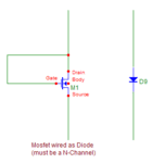
mosdiode.gif

I have on the direction of the diode.

1)since Gate is P and Drain is N, therefore the positive of the Diode should be on the Gate side? So, the picture with the diode should be reversed?

2)why it sometimes called diode load, the diode has little resistance, why it's being used as load.

3)what difference is enhancement versus depletion on the transistor?
 

1. The most significant property of a diode connected transistor is that it is always in saturation (Vds = Vgs => Vds > Vgs - Vth).
Now consider the behavior of this device. If the drain potential is higher than the source, it will be in saturation and the current will flow from drain to source, which justifies the direction of the diode in the picture.
A MOS transistor is generally symmetrical (either terminal can be drain or source). For an NMOS the terminal at the higher potential is designated drain and that at the lower potential is called source. Therefore, if the polarity of the voltage across the MOS is reversed (the terminal marked drain in the figure behaves as 'source' and vice versa), there will be no current (Vgs=0).

This explains the behavior as a diode. It only allows current to flow from drain to source if the drain potential is higher than the source potential.

2. Again, the diode load is not really an ideal diode but actually a MOS device biased always in saturation. The equivalent resistance of this can be computed easily using an AC model or you could reference any textbook ( Design of Analog CMOS ICsj by Razavi, Ch 3). For a diode load Rds ≈ 1/gm.

3. Depletion devices can be thought of as negative threshold devices. They can conduct current for zero Vgs. So in this case, the direction of the diode will be reversed (Based on the preceding logic, do you understand why?)
 
Adding on to what Calika mentioned:

1) If VDS > Vth, you get the square-law relationship between IDS and VDS (since VGS=VDS). If VDS < Vth, you get subthreshold conduction -> you can think of the FET as being open. Thus, you have current in one direction and not the other - thus a diode behavior. Of course the IV characteristic is square instead of the typical exponential for a silicon diode. Regardless, the important property is that it's blocking in the reverse direction.

2) Like mentioned by Calika, the resistance between drain and source is approximately 1/gm. This can be fairly high. Eg:
\[g_m \approx \sqrt{2(W/L)\mu_nC_{ox}I_{DS}}\]

Assuming \[\mu_nC_{ox} = 400{\mu}A/V^2, I_{DS} = 100{\mu}A, (W/L) = 20\]:
\[g_m \approx 1.26mS\]

Thus, the resistance of the "forward-biased diode" is 794Ω.

That's why it's diode-connected loading.
 

Status
Not open for further replies.

Part and Inventory Search

Welcome to EDABoard.com

Sponsor

Back
Top