Continue to Site

Welcome to EDAboard.com

Welcome to our site! EDAboard.com is an international Electronics Discussion Forum focused on EDA software, circuits, schematics, books, theory, papers, asic, pld, 8051, DSP, Network, RF, Analog Design, PCB, Service Manuals... and a whole lot more! To participate you need to register. Registration is free. Click here to register now.

How to eliminate Gate Ringing of parallel Mosfets ?

Status
Not open for further replies.

anotherbrick

Full Member level 4
Full Member level 4
Joined
Jan 10, 2009
Messages
222
Helped
1
Reputation
2
Reaction score
1
Trophy points
1,298
Location
Istanbul , Turkey
Activity points
3,190
hello dear forum,

If I want to use parallel mosfets in a half bridge to increase output current ,
( I use IR2113 for gate drive )

the mosfets blow up in few minutes after power is ON

I suspect gate ringing becouse
I read about it in some application documents

my question ;
If I use 2 seperate gate drivers for each arm of half bridge , can I eliminate this fault ?

please look at the 2 pictures for what I mean

thank you
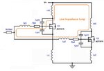
Low impedance loop GATE ringing 1.JPG
Low impedance loop GATE ringing.JPG
 

Using separate gate drivers helps a lot. Sometimes just giving each gate its own trace and series resistor is enough to isolate the two from each other. Make sure each driver has its own bypass capacitors, however.
 
The imagined "low impedance loop" through MOSFET drains isn't the primary problem, it's source inductance and possible additional inductance between sources and driver ground. Generally, separate drivers may be advantageous if the output transistors are too far apart or if suggested by the gate current magnitude. But they are useless without suitable circuit layout and correct dimensioning.

The picture is only a snippet of the full half bridge circuit, it's uncertain if the actual problem is within its scope.
 
Your pictures indicate the drain-gate loop but I'd bet the source
inductance is more the problem, if ringing is indeed the cause
of the failures. That ought to be easy enough to capture on a
'scope, being as they're low side switches and way more capacitive
than a probe tip. If you see gate ringing then go look at the source
with another probe and try to determine who's driving who.

I wouldn't be too quick to pin the blame on ringing. Could
be that gate drive is so weak that transitions are made too
dissipative (plateau at half voltage, full current had better not
persist for long). Or maybe your gate (source) ringing sets
up high amplitude drain ringing that exceeds BVdss and/or
lights up the parasitic bipolar (drain dV/dt limitations).
 
To add further insights to what other people have commented:

You are talking about a half bridge.....What is the deadtime between the turnoff of top device and the bottom turning on?
Shoot thru is a real killer in bridges (half or full), and its symptoms are as you describe, it may work a few moments, then blow up
 
Also a small 100MHz lossy ferrite bead on each gate leg will likely help, but yes symmetric tracking is vital also, if one fet has a long source track that is part of the gate drive - this will cause it to turn on last and turn off last...

keep the source to source tracks short and big, same for the gate to gate tracks... this will give you "one" device that switches together - add the gate beads (or a 1 ohm res) to limit VHF ringing...

- - - Updated - - -

looking at the gate drive with a good scope without drain power on is a good start to see if the gate drive looks good.
 
the circuit works fine with 2 mosfets

the problem is when I parallel mosfets for increasing output current

I suspect gate ringing becouse the mosfest of one or other leg blow up after couple of minutes even when there is no PWM signals but power is applied to the half bridge
 

Hi,

the circuit works fine with 2 mosfets
the problem is when I parallel mosfets for increasing output current
I suspect gate ringing becouse the mosfest of one or other leg blow up after couple of minutes even when there is no PWM signals but power is applied to the half bridge

I don´t think this is because of ringing, but it may be.

I rather think it is cause by cross conduction.
--> with paralleling of the MOSFETS you increase the total gate charge and thus you will increase switching times. This may lead to cross conduction.

Regarding one or two driver: I tend to one strong and high speed driver, but with independent gate resistors. This is a personal taste.

BTW: you speak of half bridge, but your circuit in post#1 doesn´t show a half brige configuration. This may cause confusion. With your circuit cross conduction is not possible.

Hope this helps

Klaus
 
If there are no PWM signals at the time of the fault, how can there be gate ringing??

Do you have access to a good scope?
 
- I copy pasted the schematic from an application note showing gate ringing problem
my real circuit is really a half bridge

- I didnot say that the mosfets blow up without PWM signals - I said "even when " there is no PWM signal

the mosfets blow up "also" when there is PWM signal ( inverter is running )

- I have 50 Mhz digital scope - UNI-T brand

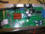
the circuit here
kart1.JPG
 

I feel the lack of the schematic with actual values of the components assembled. Anyway, sounds as the problem being due to induction of noise at wiring
 
"- I didnot say that the mosfets blow up without PWM signals - I said "even when " there is no PWM signal "

Precisely my question. Even when there are no PWM sigals, how can there be gate ringing??
 
you have bad layout , and gate traces are flowing in the air
your mosfet driver is NOT weak even though the mosfets and total gate charge is not stated (see IR2113 2.5A)
use pulldown 10k on each mosfet from gate to source ,
make sure gate drivers are not driven to 100% duty cycle to prevent bootstrap failure

and you donot need 2 drivers , you can manage up to 10 mosfets (5 on each side) for a half driver with 1 IR2113 if layout is good and gate resistors are of correct value
 
Oh yes those yellow wires for the gate drive are bad news, use a twisted pair for G & S to go from the drive to the fet (each fet) and the waveshape will improve enormously...!
 
Ringing is caused by any fast pulse with mismatched source<>load impedance.
Gate input impedance has a dynamic capacitance that rises rapidly at Vth and then drops again.

Ideal pulse can be made when you match the source s22 to the load s11. This usually involves matching Rgs and Ciss. Often diodes are sued to provide faster shutodd with a lower gate drive resistance.

Traces are often too high impedance and not controlled impedances.

Measurement methods are the most common fault of ringing.
Use the coaxial tip and barrel method with probe tip and ground lead removed between test pins ~5mm apart. If none exist, use leaded resistor wire stubs and add them and cut them short.

For long wires use AWG30 magnet wire differential twisted pairs 100mΩ /ft with as many twists as possible for low impedance (<50 Ω). This also raises capacitive load. with ~30pF /ft
 
Last edited:
sorry for my bad english - I dont mean "ringing" - I mean "parasitic oscilation"

coming to my original question ;

is it a good idea to use 2 seperate gate drive IC's for each leg of 2 parallel half bridges ?
 

the only difference in "ringing"and parasitic oscillation is the addition of positive feedback to mismatched impedance transient currents during transition.

Trace inductance and highly non-linear Ciss vs Vgs capacitance causing phase lag with EMI coupling and conductive coupling must be analyzed and controlled by design.

Coupling between channels in one IC is not a problem, but signal routing on board can be done poorly.
 
Status
Not open for further replies.

Similar threads

Part and Inventory Search

Welcome to EDABoard.com

Sponsor

Back
Top