Continue to Site

Welcome to EDAboard.com

Welcome to our site! EDAboard.com is an international Electronics Discussion Forum focused on EDA software, circuits, schematics, books, theory, papers, asic, pld, 8051, DSP, Network, RF, Analog Design, PCB, Service Manuals... and a whole lot more! To participate you need to register. Registration is free. Click here to register now.

Need a bit of help with a 12V 10A SMPS design using TL494

Status
Not open for further replies.

electrophile

Member level 2
Member level 2
Joined
Aug 30, 2013
Messages
48
Helped
1
Reputation
2
Reaction score
1
Trophy points
1,288
Activity points
1,677
I'm designing a 12VDC, 10A SMPS that would drive a brushless motor using the TL494. The motor has an inrush current of about 8A and a nominal current draw of around 5.5A. I was looking at TI's design guide here. The design example (page 24) they've done uses a 5V output (mine however would be 12V). I have two primary questions,

First: To get a 12V output, I'm guessing I would only need to change R8 and R9 divider to get the appropriate value at the error amplifier. Can I use the Vref (instead of dividing it) as one of the references for the error amplifier and then divide the 12V to 5V as the other reference for the error amplifier.

Second: The power switch seems to be a pair of NPN=PNP transistors. Can anyone recommend alternate parts for these? The NTE153 and NTE331 are not available in my part of the world. Also, can I replace this with say a power MOSFET? If so, what modifications would need to be done to power switch circuit?

Any advice would be much appreciated. Thanks!
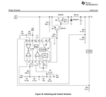
2014-03-20_135219.png
 

Can I use the Vref (instead of dividing it) as one of the references for the error amplifier and then divide the 12V to 5V as the other reference for the error amplifier.
Yes.

Second: The power switch seems to be a pair of NPN=PNP transistors. Can anyone recommend alternate parts for these? The NTE153 and NTE331 are not available in my part of the world. Also, can I replace this with say a power MOSFET? If so, what modifications would need to be done to power switch circuit?
The example design implements a complementary darlington circuit. Any combination of high power NPN (or PNP if you prefer) and medium power NPN can be used. So it's rather unlikely that you won't find suitable transistors.

Alternatively a PMOS-FET can be used, but it needs an additional Z-diode to limit Vgs to a legal range.
 
Awesome! I think the 2N3055 and the MJ3955 would work I think.

Also the document shows that the power supply is powered from a transformer whose primary is 230V AC and the secondary is 24V AC @3A. Now this is rectified through a bridge and smoothing capacitors to a 32V. Correct me if I'm wrong but the darlington combination is actually amplifying this 3A to 10A?
 
I guess MJ2955? Yes, 2955 and 3055 are fine.

Correct me if I'm wrong but the darlington combination is actually amplifying this 3A to 10A?
Amplifying isn't the right term. The circuit is forming a buck converter, which can convert a DC input voltage to a lower level with good efficiency. But the consumed input power will be always higher than the available output power.

A 24V/3A transformer (72 VA) can deliver about 50 to 55 W DC through a bridge rectifier with filter capacitor. The reduction is necessary due to limited power factor of the rectifier circuit. The calculation is for continuous load, peak current e.g. during motor start can be considerably higher. The buck converter will achieve 80 to 90 percent efficiency, so you get 40 to 50 W (12V/3.3 to 4 A) buck converter continuous output rating.
 

Thats true! The motor does have an inrush current of about 8A and a nominal draw of around 5.5A.

I was also thinking of using a 1:1 pulse transformer as an isolation between the transistor base drive and the TL494. This is what I had in mind - https://www.murata-ps.com/en/products/magnetics/pulse-transformers/78601-2c.html. I was also going to use an opto-isolator between the output voltage sense circuit and its connection to the TL494. Trying to make it a bit more safe by isolating the power and control circuitry.

I was also stuck on another point. I calculated the output inductor to be about 250uH. Consider this is a 10A supply, I figured the inductor rating would be around 12-15A. Now in my part of the world, this kind of inductor is very expensive. Hence I was wondering if using the above mentioned pulse transformer's primary winding can be used instead? It has an inductance of 500uH but I'm not sure what its current ratings are and it does not mention it anywhere in the datasheets. Can you suggest any other alternatives?

Thanks again for all your help FvM. I really appreciate it. I'll post a first-cut schematic soon.
 

Unless you have a real need for isolation, I would avoid the extra complication of that. Proper layout, power line routing and decoupling should keep things "safe".

A pulse transformer is designed for signal level currents and will not work as a power inductor.

The only way to reduce the required inductance is to operate at a higher switching frequency. What frequency are you designing for?
 

I was designing this for 20-25Khz. Also, I was told that there are some problems with the switching above 100KHz even though the device is rated till 300KHz. Is that true?
 

I was designing this for 20-25Khz. Also, I was told that there are some problems with the switching above 100KHz even though the device is rated till 300KHz. Is that true?
If you went to 100kHz the inductance would be reduced by a factor of 4-5 (required inductance inversely proportional to frequency).

At higher frequencies the losses become higher due to finite rise and fall times of the switching transistors so there's a tradeoff between frequency and efficiency. You don't want to work at the limit of the devices frequency spec so I probably won't try to go higher than about 150kHz.

Also at those higher frequencies you would want to use MOSFETs for the switches since large BJT's tend to be much slower switches (with attendant higher losses).
 

I have designed some switchers with TL494 and BJT when it was still state-of the-art, about 20 to 30 years ago. Now I would refer to MOS transistors, as already suggested. But they definitely need a push-pull gate driver to actually realize faster switching.
 

OK! Let me come back in a day or two with a schematic. Thanks a ton folks. This certainly helps.
 

I was also stuck on another point. I calculated the output inductor to be about 250uH. Consider this is a 10A supply, I figured the inductor rating would be around 12-15A. Now in my part of the world, this kind of inductor is very expensive.

You can also interleave two buck converters, using inductors rated 6 or 7 A each. It may or may not be less expensive.

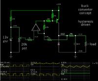
Here is a simulation of a single converter, with scope traces:


Thanks Brad! Even those are expensive too! :(

- - - Updated - - -

Attached here is a first-cut schematic.

Following crutschow's advice I changed the operating frequency to 120KHz to reduce the inductor sizeand following FvM's advice I replaced the BJT's with a MOSFET (IRFHM9331). Also I've used a MOSFET driver here (**broken link removed**) instead of the push-pull driver in discrete components. I think the driver chip does the same. I've also isolated the two feedbacks to the TL494 through opto-isolators.

Can you folks please critique this design? Maybe give me some pointers on how to make it better and more importantly if it will meet the 10A load requirements. Also how do I calculate this design's efficiency?
 

Attachments

  • TL494-revA.png
    TL494-revA.png
    115.1 KB · Views: 415
Last edited:

You can't use a regular low-side gate driver to drive a NMOS switch in a buck converter.

It's true that you need a push-pull driver for fast gate driving, but you must also observe the required gate voltage relative to source voltage. The gate voltage must swing 10 - 15 V above DC input voltage in on-state and must also keep the maximum gate voltage rating.
 

As FvM noted, you can't drive an N-MOSFET in that configuration with that driver. You need a bootstrap gate driver to get the gate voltage at least 10V above the source voltage to fully turn on the MOSFET.

You could possibly drive a P-MOSFET directly with the output of the TL-494 by exchanging the two output transistors in your first schematic with the P-MOSFET. But for better efficiency you would use the gate driver.
 
Last edited:

So if my DC voltage is 32V as in this case, the Vgs of the MOSFET needs to be 32+10=42V? Also this is a P-MOSFET. I did a basic search and found that P-MOSFETs should be driven by a non-inverting driver (which this chip is). Would I need some sort of TTL-CMOS level converter between the TL494 and the MOSFET?
 

So if my DC voltage is 32V as in this case, the Vgs of the MOSFET needs to be 32+10=42V? Also this is a P-MOSFET. I did a basic search and found that P-MOSFETs should be driven by a non-inverting driver (which this chip is). Would I need some sort of TTL-CMOS level converter between the TL494 and the MOSFET?
Yes, an N-MOSFET would need a 42V gate voltage.

A P-MOSFET gate in that circuit can be grounded to turn it on but the maximum gate-source voltage is generally 20V for most MOSFETs so you need to add a limiter for that. The P-MOSFET is turned off by pulling the gate high until it is close to or at the source voltage.

As I stated, you could likely drive the P-MOSFET directly with the output of the TL-494 by exchanging the two output transistors in your first schematic with the P-MOSFET. But for better efficiency you would use the gate driver.
 

You are right, IRFHM9331 is a PMOSFET. I didn't notice because it's wrongly connected in the schematic (S and D flipped). And you won't use a 30V transistor for 32V input voltage.

A PMOSFET works with gate voltage within the supply range, maximum Vgs must be observed though.

A standard non-inverting gate driver could be used with an auxilary supply, but unfortunately the standard drivers have an undervoltage lockout dedicated for NMOS transistors. It switches the PMOS on during supply ramping. So you probably end up with a discrete transistorgatew driver.
 
Last edited:

OK! Let me change that and come back with a modified design for the gate driver.

- - - Updated - - -

Here is a modified schematic with a totem pole driver for the P-MOSFET. Have I got this right?
 

Attachments

  • TL494-revB.png
    TL494-revB.png
    116.4 KB · Views: 377

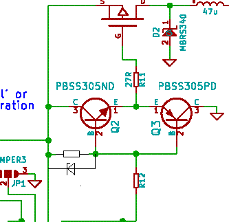
Some changes necessary, at least a pull-up resistor for the PWM output. The optional z-diode is intended to limit the gate voltage. The same purpose can be achieved by adjusting the pull-up and R12 series resistor respectively.

3298793200_1395590785.gif
 

Note also that the P-MOSFET you selected has a maximum ON resistance of 0.117Ω so the voltage drop across the transistor will be a maximum of 1.17V @ 10A. This causes an ON power dissipation of 11.7W, giving an average power dissipation of about 5W or so which will require a heatsink and significantly reduce the converter efficiency. You likely want to use a higher current MOSFET with a lower ON resistance (somewhere around 0.02Ω or less if you want to avoid using a heatsink).
 

Status
Not open for further replies.

Part and Inventory Search

Welcome to EDABoard.com

Sponsor

Back
Top