Continue to Site

Welcome to EDAboard.com

Welcome to our site! EDAboard.com is an international Electronics Discussion Forum focused on EDA software, circuits, schematics, books, theory, papers, asic, pld, 8051, DSP, Network, RF, Analog Design, PCB, Service Manuals... and a whole lot more! To participate you need to register. Registration is free. Click here to register now.

Wide band Analog time delay Circuit Schematic

Status
Not open for further replies.

crazyboy

Newbie level 6
Newbie level 6
Joined
Jan 19, 2012
Messages
12
Helped
0
Reputation
0
Reaction score
0
Trophy points
1,281
Location
India
Activity points
1,419
Hi friends can any one suggest a schematic of a wide band (30-500MHz) analog time delay circuit? I need a maximum time delay of 5ns with steps of few pico seconds. I will be very much thankful:-D.
 

Hi friends can any one suggest a schematic of a wide band (30-500MHz) analog time delay circuit? I need a maximum time delay of 5ns with steps of few pico seconds. I will be very much thankful:-D.

While in theory there may be "a circuit" to do so, you should save a block of such wideband signal in a huge memory, then delay its reading after writing.
A practical device was so far a video tape recorder which allows to record and read analog wideband signals on a tape loop. Used in VLBI since ~1975.

A "natural" way to do it is to use the propagation delay - in the air, or with a long section of a transmission line, coaxial or waveguide. Only the first allows to vary the delay smoothly, lines must be cut to a fixed length. Experiments with a "long" circular waveguide were done in the 1960s, the delay could be varied smoothly. You can try a spool of optical fiber as a suitable delay line, with a very wide "analog" bandwidth. Possibly the most versatile medium now.
 
If a mechanical adjustment is accaptable, you could use an about 1.5 m long slotted (coaxial) transmission line (that in the past was used mostly for determining phase and magnitude of VSWR to determine complex reflection coefficient (or impedance) ).

Your source comes from left, the right side you terminate (to avoid reflection). You can tap the signal via a capacitive probe (with wide band voltage division) or have probe that electrically touches the inner conductor of the slotted line. The position along the line (measured from the source) determines the delay. It can be pretty accurate and is (inherently) wide band.
 
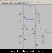
Thanks for your valuable suggestions jiripolivka. I used a schematic attached in the image file. I delayed the signal by passing through a coaxial cable of required length. I simulated its frequency response in LTspice(image also attached). My headache is that the impedance is not matching throughout the band. Up to 200MHz the VSWR response seems to be good. 200MHz-500MHz band is worse VSWR >5. Could you suggest any idea or modification in this schematic so that I can achieve good impedance matching throughout the band? Sorry for my bad English:sad:


I don't understand how your circuit or attenuation measurement can be related to VWSR without a source or load impedance?

Impedance matching will matter, if transmission lines come into play, but there are no tranmission lines, just a piece of wire (that represents zero delay in a simulation).

In my view, the circuit shows just one thing: wideband analog switching with real electronic components is far from being ideal. If I understand right, the BAT54 series resistance and diode capacitance are the only involved real circuit parameters, but sufficient to cause a considerable frequency dependent attenuation. Obviously, the performance will be worse with more than two delay steps.
 
Hi dear, I did this simulation in LTSpice. Obviously there will be attenuation depends upon the cable length and diode parameters. But in parallel I also measured its reflection loss in Vector Network Analyzer by terminating the other end with 50 Ohms and connecting the delay path with low loss cable(Times microwave LMR100). VSWR is good up to 200MHz. The LTSpice simulation also shows the 3dB cut off around 200MHz. So I messed up with these two things :roll:. Thanks for your valuable comments:). If this attenuation is not related to impedance matching, how can I achieve impedance matching for rest of band? (200-500MHz). As you told that the diode resistance and capacitance results in frequency dependent attenuation, can you suggest me a suitable diode for this requirement? The same is true for impedance matching as well? Because the LMR100 is perfect as it is impedance is well matched within the band. Please provide me a solution for matching the impedance throughout the band. I'm not bothering about the attenuation.
 

The problem would become clearer, if the simulation circuit includes source and load impedances an a tranmission line model. You can also simulate VSWR in LTSPICE if this is your parameter of interest.

I fear, there's no easy way to achieve good switch performance with BAT54 in the intended frequency range due to the diode capacitance.
 
  • Like
Reactions: WimRFP

    WimRFP

    Points: 2
    Helpful Answer Positive Rating
Hi I don't know how to do VSWR simulation in LTSPice. I Googled it and found nothing helpful. If you know how to do it can know explain briefly? Thanks in advance...
 

Consider the definition of VSWR and how the involved quantities can be "measured" in LTSpice.
 

is this for data receiver margin testing or loop stability margin test or noise test??

an All Pass Filter Design, microstrip, stripline or coax?
switch depends on test??
Can you use hot carrier schottky diodes?
 
Last edited:

Hi I don't know how to do VSWR simulation in LTSPice. I Googled it and found nothing helpful. If you know how to do it can know explain briefly? Thanks in advance...

you can "measure" reflection coefficient with the simulator. Insert an ampere meter, multiply the output with 50 Ohms and add it to the output voltage measured at the position of the ampere meter, and divide by two. Switching between adding and subtracting changes from forward voltage wave to reverse voltage wave. If the forward voltage wave has a known value (that is half the EMF), you can calculate the reflection coefficient.

If you scale the reverse voltage based on the forward voltage, the reverse voltage is the reflection coefficient. You can convert reflection coefficient to VSWR (1+|RC|)/(1-|RC|). Always check your simulated instrument with some known values to make sure you didn't make an error.

Though I didn't go through your circuit, using bat54 as RF switch up to 500 MHz is a bad idea. A PIN diode would be better. If you don't have a model, but you want to have some reasonable simulation result, just take a small signal RF schottky from the library (such as BAT15), reduce the value of RS to a value for the proposed PIN diode, increase the breakdonw voltage, and increase the TT parameter to about 500ns. This will give you reasonable results.

Though 500 MHz isn't real microwave, lead inductance can have influence, so you may add package parasitics manually .
 
  • Like
Reactions: FvM

    FvM

    Points: 2
    Helpful Answer Positive Rating
Hi I don't know how to do VSWR simulation in LTSPice. I Googled it and found nothing helpful. If you know how to do it can know explain briefly? Thanks in advance...

I can see the problem in your circuit: you ask to transmit a "wideband" signal spectrum, 30 to 500 MHz, through a delay line- in your case a cable. To transmit such wideband spectrum , your transmission line must be well matched over that frequency band, to your source and your load. Say 50 Ohms.
But your BAT54 diode switch is NOT matched to 50 Ohms, not in open state, not in closed state. Therefore your idea will not work.
I do not use simulation- experiments are more important.
What you need is not only the delay-line cable, you must include wideband matching circuits. I would recommend using a wideband MMIC amplifier at the source and at the load. Use it as an "active isolator"; amplifier input can be matched to the source by an attenuator as well as the output to a load. Amplifier gain should be set to equal the sum of those attenuators. Such devices can work in one direction and can support a wideband spectrum delay.

For the simple test you can use simple attenuators at each line end, to improve matching. Simulate what can be done. I guess a >10 dB loss must be used (5 db before and 5 dB after the delay line).

I used the described "active isolators" for a matrix of delay cables, to achieve their wideband matching, without problems.
 
  • Like
Reactions: FvM

    FvM

    Points: 2
    Helpful Answer Positive Rating
Besides pin diodes, 50 ohm matched coaxial relays would promise the best performance. It's definitely the standard solution in test and measurement applications, if switching time isn't critical. Otherwise, you should also look for GaAs analog switches.
 

@crazyboy < you are doing well to get that circuit to be flat to 200MHz.
I have no idea what this is for, but it sure looks crazy , ha!

You know all diodes are essentually "variable DC controlled caps" or "Varicaps" in reverse DC bias and different diodes are suited for different purposes. ( what is your purpose? )

"Hot carrier diodes" are use to convert RF carrier levels to DC, such as in a RF Return Loss device with DC out so you can measure with a dc voltmeter. Or if you were controlling an LC tuned circuit, you can vary the capacitance with reverse DC. Or if switching RF, you would use Pin Diodes as suggested by @WimRFP, or GaAs devices as suggested by @FvM.

But whatever the diodes are for, here, they are certainly non-linear and will create harmonics and equalization losses.
 

Hi sunny...your'e quite funny:-D. Actually my aim is to delay the signal in one of antenna's path before power combining them. This can reduce the coherence loss of signal. Now I replaced the diode, with BA482 a low resistance 1.2 Ohm and low diode Capacitance 1.2pF VHF band switching diode. The result is pretty much similar to earlier case. I decided to go with pin/ hot carrier schottky diodes as suggested by you and other friends. Let me check its response and give you the feedback :D... Thanks a lot... cheers...
 

If I understand right, you are talking about real VSWR measurements. In this case, it would be reasonable to take a look at the almost unspecified components in your schematic, particularly the inductors. Do you know their SRF respectively parallel capacitance? A usual 10 uH inductor has 50 to maximum 100 MHz SRF, in other words, it acts as a capacitor above this frequency.

You can expect down to 0.2-0.3 dB insertion loss with GaAs switches in the Sub-GHz range. I don't think that similar numbers are realistic for diodes switches.
 

@jiripolivka. I read you article on Active Isolators... very well explained. The idea of using a wideband MMIC amplifier cascaded with attenuators is promising. I'm having a doubt. My source signal is an Antenna's output which is delayed by this circuit and added with other antenna's power by a power combiner. The load is nothing but a Spectrum analyser. Do I need the same Active Isolator at Analyser side as well?
 

Status
Not open for further replies.

Part and Inventory Search

Welcome to EDABoard.com

Sponsor

Back
Top