The switching is required in many applications at low as well as at high frequency. RF MEMS switches are the specific micromechanical switches that are designed to operate at RF to mmWave frequencies. MEMS switches usages some mechanical movement to achieve a closed or open circuit in the Radio Frequency transmission lines. GaAs FET switches do not have sufficient isolations to minimize cross interference and signal jamming from channels is close proximity. MEMS switches provide high isolation when open, low insertion loss when closed, and can be operated at low power consumption. Because of electromechanical isolation, RF circuit doesn’t leak or couple significantly to the actuation circuit. MEMS are small in size hence it occupies less space in circuit designs so that which was most required device in the communicating world. Radio Frequency Micro Electro Mechanical Switches (RF MEMS) classification depends on type of actuation, deflection axis, contact type, circuit configuration, and Structure configuration. The most used RF MEMS mechanical structures are the cantilever beam and the air bridge structures. Presented design here is electrostatically actuated capacitive fixed-to- fixed bridge base capacitive switch.

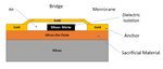
An air bridge base capacitive RF MEMS is shown here. Gold (Au) is used as a beam material, and Silicon Nitride (Si3N4) with dielectric constant 8.5 is used as dielectric material. Silicon nitride thin film dielectrics are used in capacitive radio frequency micro-electromechanical systems (MEMS) switches since they provide a low insertion loss, good isolation, and low return loss. A capacitor is built up between the fixed electrode and movable electrode. Below are components of MEMS switch
Wafer: This MEMS is fabricated on substrate as silicon, GaAs as active substrates
Bridge: Gold (Au) is used as membrane material.
Dielectric: Silicon Dioxide(Sio2) is used as insulator
Silicon as substrate

In air bridge type MEMS switch, beam is fixed at both the ends and voltage is applied in the middle of the beam to note down the displacement of the beam towards substrate. The displacement is maximum in the middle region when we go on increase the applied voltage. The actuation voltage or applied voltage or pull in voltage is the maximum voltage at which the electrostatic force becomes superior over mechanical restoring force, causes MEMS device pull down towards the ground plane. Initially the input applied voltage is 1mv there is no deformation in the switch under this condition input is equal to output, but the second case in addition a 5v is added to 1mv then there is some electrostatic force is created between the electrodes then the cantilever will deform and touches to ground under this condition the output is zero. The switch closing time depends on the actuation voltage and the opening time depends on the mechanical properties of the switch.

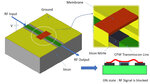
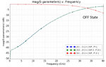
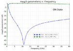
This RF MEMS Switch is designed and simulated using Finite Element Method (FEM) tool. Finite Element Method (FEM) tools are very helpful to design and simulate the RF MEMS Switch. S- Parameter results are obtained, and examine return loss (S11) and insertion loss (S12) of switches. During the OFF state the insertion loss is less than zero and return loss is less than 40 db. Vice versa output graph could be obtained during the ON state simulation of MEMS switches.

It is observed from the results that the MEMS switch circuit has an insertion loss (S21) of 0.4 dB and return loss (S11) of about less than 12 dB in the OFF state up to 20 GHz. The switch has an insertion loss (S21) of -25 dB and return loss (S11) of about -0.10 dB in the up state thus exhibiting good switch characteristics.
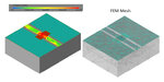
Simulated E-filed plot and FEM mesh is shown here.

An air bridge base capacitive RF MEMS is shown here. Gold (Au) is used as a beam material, and Silicon Nitride (Si3N4) with dielectric constant 8.5 is used as dielectric material. Silicon nitride thin film dielectrics are used in capacitive radio frequency micro-electromechanical systems (MEMS) switches since they provide a low insertion loss, good isolation, and low return loss. A capacitor is built up between the fixed electrode and movable electrode. Below are components of MEMS switch
Wafer: This MEMS is fabricated on substrate as silicon, GaAs as active substrates
Bridge: Gold (Au) is used as membrane material.
Dielectric: Silicon Dioxide(Sio2) is used as insulator
Silicon as substrate
In air bridge type MEMS switch, beam is fixed at both the ends and voltage is applied in the middle of the beam to note down the displacement of the beam towards substrate. The displacement is maximum in the middle region when we go on increase the applied voltage. The actuation voltage or applied voltage or pull in voltage is the maximum voltage at which the electrostatic force becomes superior over mechanical restoring force, causes MEMS device pull down towards the ground plane. Initially the input applied voltage is 1mv there is no deformation in the switch under this condition input is equal to output, but the second case in addition a 5v is added to 1mv then there is some electrostatic force is created between the electrodes then the cantilever will deform and touches to ground under this condition the output is zero. The switch closing time depends on the actuation voltage and the opening time depends on the mechanical properties of the switch.
This RF MEMS Switch is designed and simulated using Finite Element Method (FEM) tool. Finite Element Method (FEM) tools are very helpful to design and simulate the RF MEMS Switch. S- Parameter results are obtained, and examine return loss (S11) and insertion loss (S12) of switches. During the OFF state the insertion loss is less than zero and return loss is less than 40 db. Vice versa output graph could be obtained during the ON state simulation of MEMS switches.
It is observed from the results that the MEMS switch circuit has an insertion loss (S21) of 0.4 dB and return loss (S11) of about less than 12 dB in the OFF state up to 20 GHz. The switch has an insertion loss (S21) of -25 dB and return loss (S11) of about -0.10 dB in the up state thus exhibiting good switch characteristics.
Simulated E-filed plot and FEM mesh is shown here.