Continue to Site

Welcome to EDAboard.com

Welcome to our site! EDAboard.com is an international Electronics Discussion Forum focused on EDA software, circuits, schematics, books, theory, papers, asic, pld, 8051, DSP, Network, RF, Analog Design, PCB, Service Manuals... and a whole lot more! To participate you need to register. Registration is free. Click here to register now.

Widlar bandgap reference circuit Layout

Status
Not open for further replies.

rfub

Newbie level 6
Newbie level 6
Joined
Dec 9, 2009
Messages
13
Helped
0
Reputation
0
Reaction score
0
Trophy points
1,281
Activity points
1,391
Hi all, I have a layout assignment about Widlar bandgap, I have no idea about how to do it, I'm willing to learn and it's really important to my future course work.
we are supposed to layout in Cadence Virtuoso, using NCSU_TechLib_ami16 technology.
I have several questions.
1. T1:T2:T3 should be 1:10:1, what parameters in the layout can determine the ratio?
2. Is there any tutorial of picture shows how to layout a bipolar transistor?
Thank you for helping.
 

Hi rufb

Bellow there are some recommendations:

1) I agree with Keith; The layout of bipolar and diode devices are often provided by foundry, and it comes in the design kit. In every CMOS processes that I have worked, the layout of these devices was already available. And it wasn’t possible to design the layout.
2) One fundamental recommendation is to draw the bipolars in a common centroid configuration. And for this reason, it is usually preferred to use aspect ratio of 1:8, instead of 1:10. The attached figure is from my last design; you can see that all BJTs have common centroid.
3) It is also very important to match the resistors. For this, you can use the configuration also shown in the figure. Note the there are two dummies resistors.
4) It is important to choose the proper material for the resistor. It is a tradeoff between: temperature coefficient, resistance per square, matching, etc. In my design, I used P+ Poly resistor, with of TC = 160 ppm/°C

If you have another doubt, you can ask.
Palmeiras,
 

Thanks for help, however, I didn't find any pre-laid out option in cadence and we need to layout all the component by ourselves.
The attached figure is my layout, the resistor are perfectly 6k ohm and 600 ohm, the BJT transistors T1 and T2 I used the minimum size, and for T2 I just put 10 times of emitter in order to get the 1:10:1 ratio. but I think I might be wrong cuz the layout looks weird, could you please take a look at it? Thank you.

https://obrazki.elektroda.pl/40_1267676324.png
 

There will be a layout for a transistor in the PDK for the process and you MUST use that. Then you use multiple transistors for the bandgap. You DON'T do what you have drawn.

What is the process?

Also 10:1 is a strange ratio - difficult to get a good layout. Powers of 2 are better. 8:1 is good - a 3x3 matrix with the single one in the centre.

Keith
 

Hi Keith, I get quite confused because our professor never mentioned about the cadence PDK. The pdf file is an NPN layout tutorial made by our professor. We just draw the layer directly, I think the process you mentioned is about the PDK and I will go check it out tomorrow
 

As an exercise in layout, it may be ok to draw your own transistor, but in order to have models that match the layout you must use the ones in the PDK. If you want to draw a bandgap using the small transistor layout you have shown then you would just connect up 10 of those for the large transistor. You don't try to make a large transistor directly otherwise it will not electrically behave exactly like 10 individual transistors.

Keith.
 

rfub,

(a) You shouldn't draw your T2 with an emitter area 10 times bigger. You should design T2 to be 10 transistors T1 connected in parallel; as illustrated in the figure I have attached.
(b) Regarding your resistor, a good idea would be to make the matching between the resistors, as I have illustrated in the another figure that I had posted before. The way you didi, you arent matching these resistors.

Regards,
 

palmeiras, thank you, I think I understand, I will draw 10 600 ohm resistor and connect them to make the matching. But I still can figure out how can I use the PDK to get the pre laiyout. I'm using cadence virtuoso in university's server.Is it possible that they didn't install the complete tools kit?
 

Hi rfub.

About the layout of the PNP (or NPN) devices, the foundry often provides this. All design kit that I have worked, they provided this layout. So you can insert this layout directly from the library.
But it is possible that all files weren't installed. Or, it is also possible that your process doesn't have the layout already done; but in this case, as keith wrote, you will not have the electrical model for the simulation.
But I believe that you are doing a layout exercise, so... there is no problem. Do as your professor suggested.
About the resistors, you can divide each 6k resistor in 3 parts, (2000 each one), and then, you can connect its as I have shown in the first posted figure I. (interdigitated)
ok?
Regards,

Palmeiras
 

However, you could add the layout of transistors (MOS and BJT) or resistors, directly using Virtuoso L layout. There is no need to use XL. Off course, the XL version presents a lot of more features and it does this insertion automatically.
But using L version, you ncan insert manually. Althought it works too.
Maybe you XL version is not configured or, There is missing files in your design kit installation.

Regards,
 

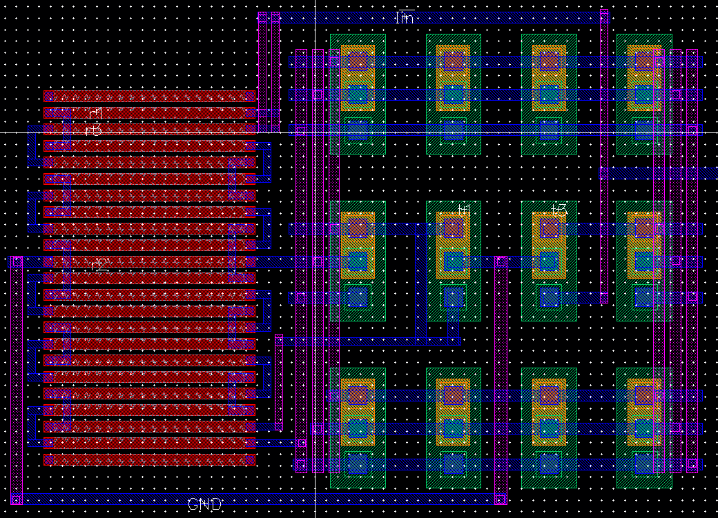
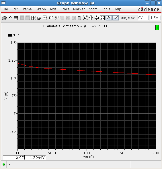
I want to thank all of you, I just finished the layout, the simulation result is perfect, here are my layout view and the spectre plot.

52_1267819243.png


9_1267819244.png
 

The simulations don't look great - the voltage is too low and the temperature coefficient is poor. Are you sure you have the resistor values correct?

Keith.
 

The reference voltage should be around 1.2 volt by calculation. What does it mean the emperature coefficient is poor? yes each segment of resistor is 600 ohm.

**broken link removed**
 

The layout is nice!
He said that the coefficient is poor, because the curvature of your output voltage is not parabola. Please, measure how much your reference is varying in a function of temperature.
To correct this you must do adjust in the value of resistors aspect ratio. ok?
regards,
 

rfub said:
The reference voltage should be around 1.2 volt by calculation. What does it mean the emperature coefficient is poor? yes each segment of resistor is 600 ohm.

**broken link removed**

The characteristics should look like this, plotted at the same Y scale as yours:

Your resistor ratios are wrong.

Keith.
 

Status
Not open for further replies.

Similar threads

Part and Inventory Search

Welcome to EDABoard.com

Sponsor

Back
Top