Continue to Site

Welcome to EDAboard.com

Welcome to our site! EDAboard.com is an international Electronics Discussion Forum focused on EDA software, circuits, schematics, books, theory, papers, asic, pld, 8051, DSP, Network, RF, Analog Design, PCB, Service Manuals... and a whole lot more! To participate you need to register. Registration is free. Click here to register now.

Why this topology is called a comparator?

Status
Not open for further replies.

zhangseong

Member level 2
Member level 2
Joined
Sep 22, 2006
Messages
44
Helped
0
Reputation
0
Reaction score
0
Trophy points
1,286
Visit site
Activity points
1,563
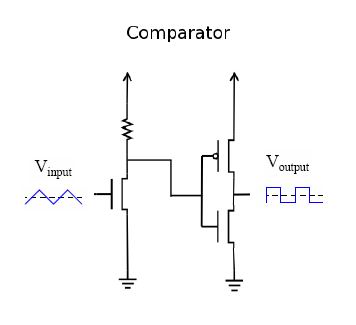
why is this topology is called a comparator ? how the circuit perform , what is the 1st part of the circuit ? is it an inverter?
18_1174449067.jpg
 

Re: comparator

Can you please specify where are the two inputs...Of course the last part of the circuit is a cmos inverter....
 

Re: comparator

maybe the reference voltage is regarded as the MOS threshold.
the first stage is a pre-amplifier stage
 

Re: comparator

the first stage is the resistively loaded comon source amplifier stage.
 

comparator

it's a single-Ended comparator. it 's just is a buffer.
the threshold of comparator(not nmos) varies along with process!
 

comparator

If you need to regard this as comparator, then the trip point is the inverter trip point where it can switch from L to H. Then first stage determines when to turn over when the INPUT is switching from VSS to some point (say, VDD/2) where parallel equivalent resistance of the RDS of NMOS and the up resistor is equal to the trip point of inverter, then the inverter turns from L to H, that's the comparison happens.
 

Re: comparator

hung_wai_ming(at)hotmail.com said:
If you need to regard this as comparator, then the trip point is the inverter trip point where it can switch from L to H. Then first stage determines when to turn over when the INPUT is switching from VSS to some point (say, VDD/2) where parallel equivalent resistance of the RDS of NMOS and the up resistor is equal to the trip point of inverter, then the inverter turns from L to H, that's the comparison happens.

Hi,

As we know that the trip point of a inverter is VDD/2, then in order to be the trip point voltage, the common source amplier effective dc voltage is designed at VDD/2. Then as the common source dc voltage increase or decrease from VDD/2 will trigger the inverter either to be in logic high or low.

Thx
 

Status
Not open for further replies.

Similar threads

Part and Inventory Search

Welcome to EDABoard.com

Sponsor

Back
Top