Continue to Site

Welcome to EDAboard.com

Welcome to our site! EDAboard.com is an international Electronics Discussion Forum focused on EDA software, circuits, schematics, books, theory, papers, asic, pld, 8051, DSP, Network, RF, Analog Design, PCB, Service Manuals... and a whole lot more! To participate you need to register. Registration is free. Click here to register now.

Why is gate and drain not shorted in digital design

Status
Not open for further replies.

ojha

Newbie level 3
Newbie level 3
Joined
Mar 14, 2014
Messages
3
Helped
0
Reputation
0
Reaction score
0
Trophy points
1
Activity points
27
we say that we require Ioff to be as low as possible and Ion to be as high as possible.... wouldn't then it be wise to short source and drain... so that we get conduction only when there is gate voltage, otherwise no current.. we can have Ioff as zero... why don't we do this in digital design...
 

Hi ojha,
pls be specific in yr qn or which digital u r meaning?
And can u pls confirm, u wish to short Source and Drain or Gate and Drain?

It is not not necessary that "Ioff to be as low as possible and Ion to be as high as possible.... "
MOSFET is a switching device, Depending on our application. It varies.

Regards,
Shunmuga Sundaram


Thanks for responding, Shunmuga Sundaram
Sorry, I meant shorting drain and gate.....
digital applications means logic design where we just need '1' and '0' states..
wouldn't it be better if we jus had 0 ioff so that we have min power consumption...
why is this configuration not used.... because all we want is "conduction" or "no conduction"
 

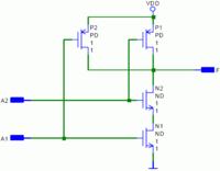
See below a simple digital CMOS circuit, a two-input nand gate.


Where do you want to short drain and gate, or maybe gate and source, and what do you want to achieve?

The circuit as-is will do what you claim, turn fully and and off, by nature of the design and without additional means.
 

See below a simple digital CMOS circuit, a two-input nand gate.


Where do you want to short drain and gate, or maybe gate and source, and what do you want to achieve?

The circuit as-is will do what you claim, turn fully and and off, by nature of the design and without additional means.


In this case also, there will be finite off current (as current in subthreshold region is not exactly zero)... which is a parameter that needs to be lowered as we are scaling down the technology...
my point is... why can't we just short the gate with vdd supply...
would we not get the desired output... with the advantage of no leakage current ioff
 

Yes, a source-drain short in one gate state and a
source-drain open circuit in the other would be ideal.

You can't have ideal. Not on the menu, not at any
price. So while you're at it you may as well ask for
zero gate charge and zero drain capacitance, an
infinitely sharp subthreshold region and all the other
perfect and unattainable attributes you can imagine.

Then, accept that you get to choose among what's
real and available, and get on with the design without
the benefit of fantasy elements.
 

Are you sure that such a "stuttering" is in accordance with our forum rules?
Most of us do not bother trying to translate text speak "stuttering" from a little kid with a cell phone.

I have never seen "qn" before. Is it "question"?
 

Are you sure that such a "stuttering" is in accordance with our forum rules?

Forum rules:

Post content described below is not allowed:
..........
..........
SMS abbreviations, they make posts unreadable and prevent many users that don’t know English well enough to understand them. Type complete words.
 

Hi ojha,
Thanks for your confirmation.
As of my knowledge, We will be shorting Gate and Drain of the MOSFET (similarly Base and Collector in case of Transistor) to operate in Diode mode. Usually for temperature sensor ckt applications, we have these kind of configurations, because in case of temperature sensors, the value of increased temperature is determined from the drain current / collector current values which are dependent on temperature values.

I think this may be useful.

Pls let me know if you need any other details.

Regards,
Shunmuga Sundaram
 

Status
Not open for further replies.

Part and Inventory Search

Welcome to EDABoard.com

Sponsor

Back
Top