Continue to Site

Welcome to EDAboard.com

Welcome to our site! EDAboard.com is an international Electronics Discussion Forum focused on EDA software, circuits, schematics, books, theory, papers, asic, pld, 8051, DSP, Network, RF, Analog Design, PCB, Service Manuals... and a whole lot more! To participate you need to register. Registration is free. Click here to register now.

why are some ground/power planes done with a "grid" flood pattern?

Status
Not open for further replies.

Roger Freeman

Junior Member level 2
Joined
Jan 19, 2008
Messages
23
Helped
5
Reputation
10
Reaction score
5
Trophy points
1,283
Activity points
1,556
Hello

For RF designs I have always specified a "solid" copper flood for ground and power planes, with sparing use of thermal reliefs if necessary (and avoided them for RF!).

However, I note that a lot of consumer/professional PCBs have planes like this:
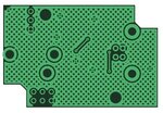
ground_plane.jpg
**broken link removed**
pcbtrace20_new.jpg
https://rayshobby.net/wordpress/wp-content/uploads/2013/05/pcbtrace20_new.jpg

whereby the copper fill is divided up into a grid rather outcome than being solid. I don't know why this is done - for a start off, it presumably takes longer to manufacture because it requires more etching, and it uses up more of the etchtant and prolongs the board's exposure to the etch process (with resultant undercutting of tracks being the likely risk).

So what's the advantage of using these "cross-hatched" or "gridded" or "checkerboard" floods? Is there a proper name for it?


RF
 
Last edited by a moderator:

I believe that it is called "thieving". It is done to help with even heating of the board during reflow. It also supposedly helps with warping of the boards during reflow.

I'm with you... I have always used solid ground pours and I NEVER used thermal reliefs for my RF designs. The manufacturing engineers used to screem bloody murder when I told them "no" to thermals. I even provided evidence that thermals effected the frequency response of the signal. They hated it, but thermals were NOT used. They always said that yields would suffer, but it turned out that this was not the case. Better profiles took care of most of the uneven heating issues during reflow.

Ahhh ...yes, that makes sense. I hadn't thought of that at all. "Thieving" ... got it! Thanks very much.

Yes, my designs have caused consternation too, just like you've experienced, but with a decent process you can still get non-thermally-relieved things to "take" and the company hasn't gone broke so I guess our yield's OK!

Thanks for solving my miniature mystery.

RF
 

I believe that it is called "thieving". It is done to help with even heating of the board during reflow. It also supposedly helps with warping of the boards during reflow.

I'm with you... I have always used solid ground pours and I NEVER used thermal reliefs for my RF designs. The manufacturing engineers used to screem bloody murder when I told them "no" to thermals. I even provided evidence that thermals effected the frequency response of the signal. They hated it, but thermals were NOT used. They always said that yields would suffer, but it turned out that this was not the case. Better profiles took care of most of the uneven heating issues during reflow.

Totally Wrong.
It is not thieving it is a hatched ground pour... There are connections to pads for a start off. Hatched copper was popular in some instance because of misunderstandings of how a ground plane functions and some myths regarding eddy currents...
The rest regarding reflow is a bit misinformed...
Thieving is added to a design to even out the copper deposition during the plating process to avoid isolated areas of copper becoming over plated.
You can reflow boards with no copper planes or boards with many copper planes you do not put copper planes inside a board to spread the heat during reflow!
As to thermal reliefs I have had boards made with 4 and 6oz copper with no thermal relief, again its down to profiling a board correctly for reflow.
 
I agree with marce, thieving is more of a process to add dummy copper shape to balance out the board as unbalance boards sometiomes result in warping. This dummy copper doesnot require to be associated with any net though.

Where as grid pattern or more approprately calle hatched copper is used in flex pcb to keep it flexible as solid copper results in little stiffness of flex PCBs.
Earlier there used to be dry soldering issues due to solid copper, but as marce said, with today's manufacturing capabalities there us no issue.
 

It also makes life a lot harder, when you route the board and then pour copper and make it hatched - you can guarantee that there will be some vias that either fall between the hatching or do not connect to it as fully as the designer would want.

Although another suggested benefit of it is reduction in weight as you reduce the amount of copper and if the board is so weight crucial that every little thing helps - this can.
 

No good for a contiguous return path for signals though.... outdated outmoded design practice...
 

I can't think of a single reason why a grid pattern would have superior characteristics than a solid plane.
 

Its old school, 1980's where some worried about eddy currents on a solid plane, if I ever get chance I will search through my old documentation, it was when we had less empirical data on ground planes and these sort of myths (90 degree corners was also around at the time and still persists) abounded PCB design and layout......
 

90 degree corners was also around at the time and still persists, abounded PCB design and layout......
Perhaps the reason for that was that 90° angles look ugly compared to 45° angles? I still prefer 45° unless it's really high speed simply because in my opinion it looks better on the board.
 

I prefer 45 angles but 90 degree angles are good into the GHz range.....
What many forget is every via is a 90 degree bend for the signal, ref Howard Johnson.
 

I prefer 45 angles but 90 degree angles are good into the GHz range.....
What many forget is every via is a 90 degree bend for the signal, ref Howard Johnson.
I usually try to avoid vias in RF traces for this reason, but perhaps that's another wrong idea of me?
 

Status
Not open for further replies.

Part and Inventory Search

Welcome to EDABoard.com

Sponsor

Back
Top