Continue to Site

Welcome to EDAboard.com

Welcome to our site! EDAboard.com is an international Electronics Discussion Forum focused on EDA software, circuits, schematics, books, theory, papers, asic, pld, 8051, DSP, Network, RF, Analog Design, PCB, Service Manuals... and a whole lot more! To participate you need to register. Registration is free. Click here to register now.

Why are R,C,L component footprints different sizes, when I select same size packages?

Status
Not open for further replies.

skatefast08

Full Member level 4
Full Member level 4
Joined
Jan 24, 2018
Messages
191
Helped
2
Reputation
4
Reaction score
2
Trophy points
18
Activity points
1,800
It dawned on me, when I selected the same size packages (0402) for resistors, capacitors, and inductors, each different component aspect (R's, C's, and L's) looked a different size, even when each component I selected were 0402. I selected 0402 Murata inductors, 0402 Murata and AVX capacitors, and for simplicity I just used, R-US _R0402 resistors and just placed the value in. Now, for some reason, the outer rectangle (red; top layer) for the capacitor will look the smallest, the inductor would be middle sized, and the resistors would look really big. Why is this? Should I be worried that my components placed in the pcb design will not overlap or be too far from each other when I place the different sized components on the board; this could result in a different dimensions on the actual board, right?
 

Hi,

with your given information ... what answer do you expect? Mine is: "Yes, no, maybe"
We don´t know what software you use, nor what libraries you use.
We don´t see t your screenshot. .. and no dimensions.

Klaus
 

Every manufacturer has their own preference.
The best way is to use their given information on footprint dimensions.
 
Hi,

with your given information ... what answer do you expect? Mine is: "Yes, no, maybe"
We don´t know what software you use, nor what libraries you use.
We don´t see t your screenshot. .. and no dimensions.

Klaus

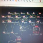
Sorry, I should have told you about the software, I am using Eagle. I pasted a photo of the board layout here (I had to take a pic of it with my phone, because I am on another computer and cannot access internet with my personal computer, so its not as clear as a screen shot):

3gLCdBw.jpg

As you can see, the capacitors are the smallest, the inductors are next biggest, and the biggest are resistors. Are the resistors, capacitors, inductors suppose to be the same size (0402)? Ignore C7 though, I was thinking I might need a bigger capacitor for the input of 9v to the regulator. I am designing an LNA.
 

Could have to do with the endcaps and the molding,
some "reach under" further than others. For resistors,
may have to do with guidance for power dissipation /
self heating (expect lands would be larger for a more
robust attach at locally elevated temp).

But why the "why?"? Are you going to go off in the
bushes to make your own footprints to save a square
millimeter?
 
But why the "why?"? Are you going to go off in the
bushes to make your own footprints to save a square
millimeter?

I was thinking If I lose a millimeter I could short the circuit on accident, because I would have thought the component looked smaller on the CAD drawing, when its suppose to be bigger and might short something or will increase parasitics (working at 2 GHz). Will PCB manufactures check to see if something is short and will fix it for me? But I will go as it is and take your word for it, this is my first microwave amplifier and PCB design. Thanks
 
Last edited:

Hi,

It really doesn't look like they all are 0402 size.

Klaus
 

Many CAD libraries are using unified footprints for industry standard packages like 0402, 0603 etc., ignoring manufacturer specific suggestions. According to IPC, different footprint sizes for different design densities are suggested.
 

It is because the termination of them is all different.
I.E. If you look at a resistor, it has metalic coating around the end only yet a capacitor may have it surrounding the complete end (top/bot, end, sides)

Inductors too have a different termination than say resistors.
So they need different solder profiles, different fillets, side fillets not just end etc.

Then there are different soldering methods, wave, reflow etc.
Then you have different densities, smaller footprints because the board is having more stuffed onto it, its higher volume, perhaps larger footprints for higher reliability (mil spec/medical).
Then you have different engineers views on it.

Then your piece of string has different lengths.

Hence different footprints. :)
 
  • Like
Reactions: d123

    d123

    Points: 2
    Helpful Answer Positive Rating
Status
Not open for further replies.

Part and Inventory Search

Welcome to EDABoard.com

Sponsor

Back
Top