Continue to Site

Welcome to EDAboard.com

Welcome to our site! EDAboard.com is an international Electronics Discussion Forum focused on EDA software, circuits, schematics, books, theory, papers, asic, pld, 8051, DSP, Network, RF, Analog Design, PCB, Service Manuals... and a whole lot more! To participate you need to register. Registration is free. Click here to register now.

why a brief copper blocks are put on the either side of transmission line?

Status
Not open for further replies.

wangzhao

Newbie level 5
Newbie level 5
Joined
Sep 28, 2022
Messages
8
Helped
0
Reputation
0
Reaction score
0
Trophy points
1
Activity points
52
Hi, everyone.

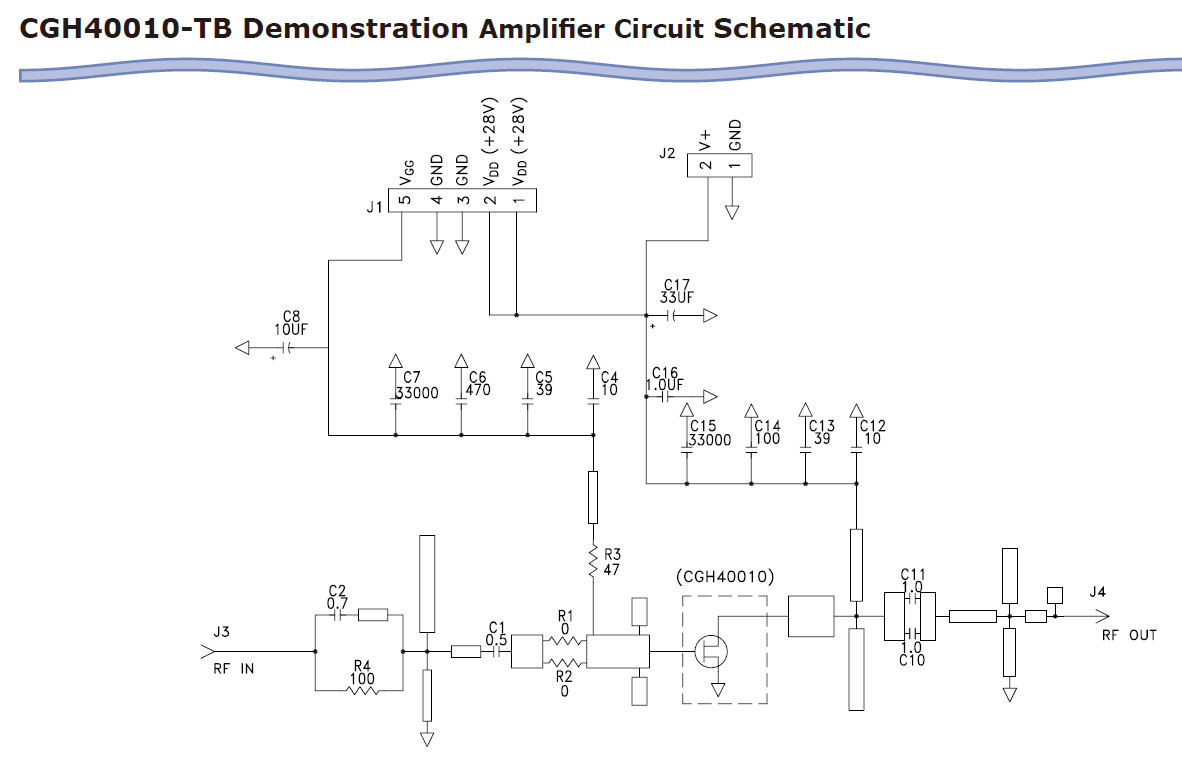
I am getting through CGH40010 datasheet.
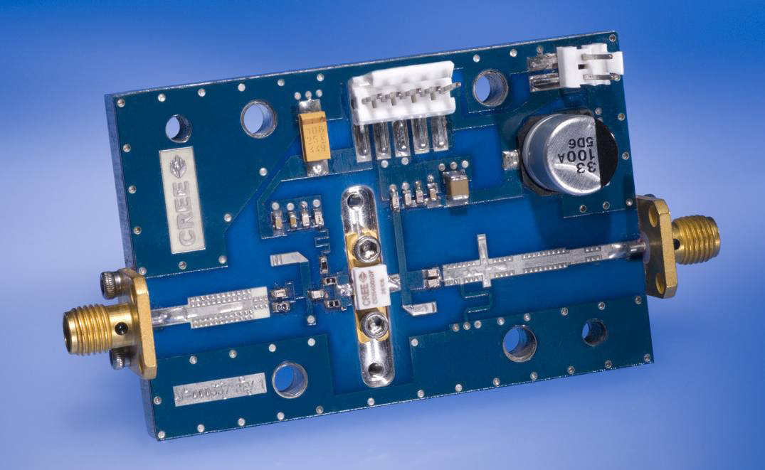
It gives a demonstration circuit diagram, the transmission lines link input and output SMA port.

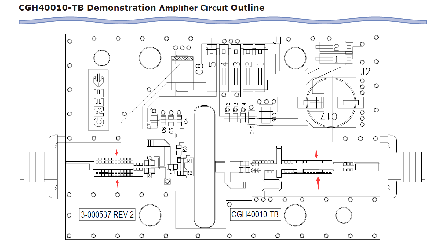
And why it add copper pads on the beside?
( the red arrow )
1673341232017.png
1673341279435.png


1673341439952.png
 

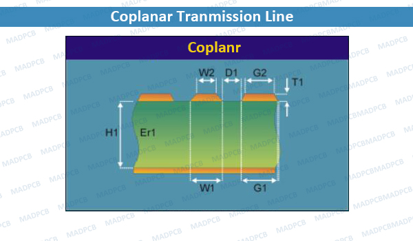
Coplanar wave guide... That's how it's routed, pretty common with rf/microwave signals...

Basic stuff:
 

Hi, marce.
The stack up model you post shows that the ground strips on the left and right side has some distance from trace.
But in CGH40010 datasheet circuit, its little copper blocks almost stick to transmission line.
Why is it designed in this way?
 

As you stated yourself the purpose is impedance tuning of the input and output matching circuit. It's performed by bridging individual copper squares either to adjacent transmission line or waveguide ground pour.

The same technique can be also found with pure microstrip lines without embedding ground.
 

Hi,FvM.
If the little copper squares aim to be soldered manually, in the circuit pic, the squares and the stripline share the same tin surface. Have them been bridged? Has the copper square been connnected to the ground?
 

I presume, the squares are initially unconnected. You'd review the evaluation board gerber or original PCB to know for sure. I mentioned an option to connect squares to ground, but it's apparently not intended in the evaluation board because ground is covered with solder mask.
 

For me it seems;
1- in one port like a quarter-wavelength matching
2- in the other port a matching network includes at least one parallel capacitor and one parallel inductor made by microstrip lines (and also maybe some LC resonators!).
Anyhow, they used some special techniques using that copper/tin blocks.
 

Status
Not open for further replies.

Part and Inventory Search

Welcome to EDABoard.com

Sponsor

Back
Top