Hi
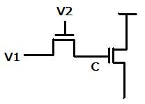
Voltage at node C would be V(V1)+q/C, where
q= charge injected by transistor V2;
C= capacitance at node C;
If transistor is of NMOS type than q would be negative - so resultant voltage would be lower than V(V1).
I think that: voltage at node C will be a little bit less than VDD due to the charge injection but enough to keep transistor in the right side on (i. e. VGS higher VT)
1) If V1 and V2 is VDD, so both transistors are ON, and node_C is ~ (VDD - VTH_n). Where VTH_n is the threshold voltage of NMOS.
2) If V1 is VDD and V2 is gnd, so, node_C is a little bit less than (VDD - VTH_n) due to the charge loss. Therefore, transistor in the rigth is still on.
You can check this in my simulations using 0.18 um technology and VDD = 1.8.
I hope the explanation is clear now. If you have other concern, you can post it again.
The figuring of q, is always tricky. Up until the point
that the channel "goes away", the gate charge will
be returned to the (presumably stiff) V1 with the G-S
portion of charge bleeding back at an RC limited rate.
It is not Q=cox*(VH-VL) in the end, because of this.
A charge-conserving model and one well fitted to
(this wafer & lot's) reality is wanted.