Continue to Site

Welcome to EDAboard.com

Welcome to our site! EDAboard.com is an international Electronics Discussion Forum focused on EDA software, circuits, schematics, books, theory, papers, asic, pld, 8051, DSP, Network, RF, Analog Design, PCB, Service Manuals... and a whole lot more! To participate you need to register. Registration is free. Click here to register now.

What is the reason for MOSFET burning?

Status
Not open for further replies.

ratheeshvaram@yahoo.com

Junior Member level 3
Joined
Oct 17, 2013
Messages
29
Helped
4
Reputation
8
Reaction score
4
Trophy points
8
Activity points
209
hai every one,
I am designing a variable inverter, output- 100V-300V, (40Hz-70Hz) 10W and input-12V,1A. for this I chose one DC-DC converter and DC-AC converter.
my first step is to get a max. DC voltage from DC-DC converter, give the output of this converter to the supply voltage of MOSFET in DC-AC converter Hbridge, provide a SPWM signal according to the desired output AC voltage, and finaly design a filter to get pure AC wave.

in DC-DC converter: I use pushpull topology (50Khz) , PIC16F716, IR2113 (driver), IRF3205 (MOSFET). the outpout of transformer is fed to the bridge rectifier (UF4007) and finally to a filter 47uF/400V. I got the output as ~400VDC, when i connected an LED through 200K resistor.
-duty cycle is 50%.
-10K is used form gate to ground
-using a 0.01uF and 56ohm (snubber) in parallel to primary.

In the DC-AC converter: I use full bridge topology (30KHz), PIC 16F716, IR2113 (driver), IRF830 (MOSFET). I use only 60 devision for sin wave generation. when I am connecting 12V in place of MOSFET supply, I am getting a SPWM signal across a 1K resistor, and nearly 8V AC on multimeter.

But when I connected the DC-DC converter output to MOSFET supply, the two MOSFET in one side of H Bridge burned.
I used 22uF/50V (electro) in parallel to 0.1uF as bootstrap cap.
-the load is 1K resistor
-the ground is common for entire circuit.
-12K is connected from gate to source.
-no snubber connected.

-uploading the schematic is not easy as we have to follow many company. rules, But I had verified the circuit of both DC-DC and DC-AC converter with many EDABOARD blogs...

friends what will be the reason for MOSFET burning...???
is any one feel something wrong in above explanation???
 

Re: Need help in inverter design

We can't really understand your problem without the circuit diagram but as for the burning of the mosfet it means their will be possible cross conduction between the high and low mosfet, but to get it clear the circuit will help us to know the exact problem...
 
Re: Need help in inverter design

thank you, kabeer and amayilsami,
I understood the need of posting circuit, I am trying to get permision. I had two doubts,
-in H bridge circuit I had used DFP740 (High sides) and IRF 830 (Low side), will it be a reason of cros conduction
-in H bridge low side, I didnt use use UF4700 across gate resistor, but in high side I had used it......
 

Re: Need help in inverter design

Many people are ready to help but we can really do anything as we don't know how your circuit is for now,and i dont know why you decide to use different mosfet between the low side and high side?
 

Re: Need help in inverter design

Many people are ready to help but we can really do anything as we don't know how your circuit is for now,and i dont know why you decide to use different mosfet between the low side and high side?

in my company getting desired components will take much time. so i tried to adjust with existing components.
 

Re: Need help in inverter design

Many people are ready to help but we can really do anything as we don't know how your circuit is for now,and i dont know why you decide to use different mosfet between the low side and high side?

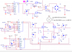
here is my circuit......
 

Attachments

  • ps.png
    ps.png
    35.3 KB · Views: 397

Re: Need help in inverter design

kabeer,
still the problem is there, DC-DC converter is working indipendent, DC-AC converter working with 12V.. but when connecting DC-DC output to DC AC converter as Mosfet voltage two MOSFET on one side is burning... it damages the driver and PIC microcontroller..please help me.......
 

Re: Need help in inverter design

ok lets do it this way your circuit diagram looks ok but one more thing i am suspecting is their is a problem hanging some where may be from the micro-controller,try and build separate oscillator for DC-DC side,did your inverter uses feedback?if so send the screen shot of the signal from the micro-controller please....

kabeer,
I am using two microcontrollers, one for DC-DC and other for DC-AC,
I doubt, in the high side the switching freq is 30KHz, but the bootstrap capacitor I chose from Tahmids blog (in that high side was 50Hz),
so instead of using below 100nF capacitor I used 22uF,
if it is so it will cause the cross conduction...????
 

Re: Need help in inverter design

ok lets do it this way power your DC-DC converter and test it with load like 100w bulb and give me the result
 

Re: Need help in inverter design

hello Yahoo.com.

can i ask you one... this inverter for what application ? is it for inductive load ? resistive load ,,for what ?.

then i am finding on your circuit , Mvolt ground is tie up with your +12v ground , this is may be creating problem , please check .
madhu hegde

this is to test our product, which is using transformer less power supply
if I did'nt tie up Mvolt ground with +12V, the gnd of ir2113 and MOSFET will become different, no?, then MOSFET will switch well?...
 

but what about your controller GND ? that also tied up with Mvolt gnd ?
 

DFP740 transistor has too low VDSS voltage. So i think it conduct current even when it gate is not drived. And it cause shoot-thru currents when low side MOSFET is driven .
You must use transistor with VDSS voltage at least 500V (IRF830 for example).
 

ok,
But I make all 4 MOSFET IRF830 (same as in circuit), cecked DC-DC converter (getting 400V, with LED as load) , checked DC-AC converter using 12VDC, getting an AC without filtering... and when I connected dc-dc output to mosfet voltage the same thing happened only after 10s (10s, because after 10s only I started SPWM signals for H bridge..) until that I had got the 400VDC from DC-DC converter...

n high side I am giving 30KHz and low side 40-70Hz
all ground are connected together..

what things caused the cross conduction, please help me
 

dead time using program...

first it was nearly 100us and because of this program.. I changed to 1ms... (to check is it the problem of dead time..)
 

So try my solution for preventing H-bridges burning while testing:
ps.png
Connecting bulb before bus capacitor (for example in the rectifier input in AC powered H-bridges) not prevent MOSFETS.
This prevent.

If bulb (bulbs in Yours example) blinks You have strong Cross-Conduction.
But often bulb not blinks although cross-conduction occurs. This is becouse cross-conduction take short part of time. So measure voltage on Q3 and Q5 Drains by oscilloscope. Voltage should not falls to much. If falls, You have cross-conduction.

PS. You have very low-power DC-DC converter so maybe use low power bulbs, for example 10W.
 
Last edited:

Status
Not open for further replies.

Similar threads

Part and Inventory Search

Welcome to EDABoard.com

Sponsor

Back
Top