Continue to Site

Welcome to EDAboard.com

Welcome to our site! EDAboard.com is an international Electronics Discussion Forum focused on EDA software, circuits, schematics, books, theory, papers, asic, pld, 8051, DSP, Network, RF, Analog Design, PCB, Service Manuals... and a whole lot more! To participate you need to register. Registration is free. Click here to register now.

[SOLVED] What is PCB Heat sink copper area??

Status
Not open for further replies.

mamech

Full Member level 3
Full Member level 3
Joined
Nov 9, 2010
Messages
176
Helped
0
Reputation
0
Reaction score
0
Trophy points
1,296
Activity points
3,135
hello


I am newbee in the field of pcbs, and I was implementing a ready-made power supply design, and I have encountered this:
"52 mm² area on Copper PCB. 2 oz (70 µm) thickness. Heatsink for use with Device U1."


my questions are:
1- how will this copper area look like? it is printed? or it is an external component that i need to buy?
2- how to do this on pcb software?
3- how this area will sink the heat? how the device will dissipate heat in it?


thanks
 

1- how will this copper area look like? it is printed? or it is an external component that i need to buy?
2- how to do this on pcb software?
3- how this area will sink the heat? how the device will dissipate heat in it?

It can be PCB solid copper area 7X8mm, preferably on both sides, connected with 4-8 solid via (via filled with solder)

It should look like a big pad that will connect with the heat sink embedded in U1 and connected with solder; if you look under the dev U1, that should have the solid copper block

Most likely your PCB will have 1 oz thickness of copper; you can increase the area in that case

Design the copper area so that most of the device heat sink overlaps the copper and 50% or more of the copper area should be exposed

Obviously no solder mask and no silk screen on this area

Draw a copper rectangle using your favourite PCB design software

Solder the device heat sink to this PCB heat sink.

Look up some professional PCB and you will understand. Vias will conduct heat to the other side
 
  • Like
Reactions: mamech

    mamech

    Points: 2
    Helpful Answer Positive Rating
Hi,

You say "U1"..
The device usually has a name...and a datasheet.
In the datasheet you should find those informations.
Either in the datasheet or in extra documentation there should be a pcb layout design guide.

Klaus
 

It should look like a big pad that will connect with the heat sink embedded in U1 and connected with solder; if you look under the dev U1, that should have the solid copper block

thank you very much for these information.

one more question. what kind of material used for soldering the component embedded heat sink to the pcb copper area heat sink? silicon paste? or normal soldering with Sn/Lead wire?
 

Hi,

what kind of material used for soldering the component embedded heat sink to the pcb copper area heat sink?
The heatsink IS the PCB copper, no need to solder.


Klaus
 

Hi,

You say "U1"..
The device usually has a name...and a datasheet.
In the datasheet you should find those informations.
Either in the datasheet or in extra documentation there should be a pcb layout design guide.

Klaus

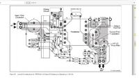
This is the proposed pcb layout for U1. U1 is TO264EG from power integrations.


I can see in the photo of pcb that the heat sink is not on copper, but it is an external heatsink.
can I use external heatsinks instead of copper heat sink area?

thanks
 

The PCB pattern clearly shows one big heat sink HS1 to be used for U1. The device does not use PCB copper as heat sink (it produces too much heat). It has both the control and driving transistor integrated. Use a big and good heat sink for this device.
 
  • Like
Reactions: mamech

    mamech

    Points: 2
    Helpful Answer Positive Rating
Hi,

You really make it difficult for us..

The true partname is: TOP264-EG... so it is hard for us to find the datasheet.

Then once you open the datasheet you see the device comes in different packages... some for PCB as heatsink, some for extra heatsink.

On the first page you see a short package description "Advanced package options" It gives a brief information about heatsink options.

Additionally you find a section called "Heat sinking"
....and a PCB example design for each package, where you clearely can see the described copper areas / heatsinking methods.

What more information do you need?

Klaus
 
  • Like
Reactions: mamech

    mamech

    Points: 2
    Helpful Answer Positive Rating
It can be PCB solid copper area 7X8mm, preferably on both sides, connected with 4-8 solid via (via filled with solder)


Most likely your PCB will have 1 oz thickness of copper; you can increase the area in that case

You cannot just replace 2oz with 1oz copper and increase the area, the heat spreading effect of thin copper has to be taken into account, this is not very good for 1oz copper... Look up the figures, after a certain distance the copper is redundant.
 

Status
Not open for further replies.

Part and Inventory Search

Welcome to EDABoard.com

Sponsor

Back
Top