Continue to Site

Welcome to EDAboard.com

Welcome to our site! EDAboard.com is an international Electronics Discussion Forum focused on EDA software, circuits, schematics, books, theory, papers, asic, pld, 8051, DSP, Network, RF, Analog Design, PCB, Service Manuals... and a whole lot more! To participate you need to register. Registration is free. Click here to register now.

[SOLVED] Waveshaping circuit - want symmetrical rise and fall

Status
Not open for further replies.

d123

Advanced Member level 5
Joined
Jun 7, 2015
Messages
2,505
Helped
494
Reputation
992
Reaction score
525
Trophy points
1,393
Location
Spain
Activity points
27,148
Hi,

Further to Dana's observation in another thread (about my adjustable brightness torch circuit) that the human eye sees a linear increase as not linear, but does see an exponential increase as a linear one, I am trying to re-shape the capacitor charge voltage to emulate this. Instead of the current source and current sink (which I also have reservations about using in the circuit as I know they will have issues across temperature related to faster and slower capacitor charging) to make a linear capacitor charging function, I'm looking to create an exponential rise and fall of the capacitor voltage, if that's feasible.

I've tried different things on paper and tried to reason out what could work and then tested the ideas in simulations (as I can't probe the signal at present with my oscilloscope nor guage it with my eyes nor measure it meaningfully with a DMM on a breadboard version) using various BJT configurations, some with RC waveshaping on the bases and collectors and/or emitters - quite the Christmas Tree full of decorations... - but it seems the simplest circuit of all with no RC delays anywhere produces the same result as any of the more complex circuits with RC delays and so on, so this is where I am with the idea:
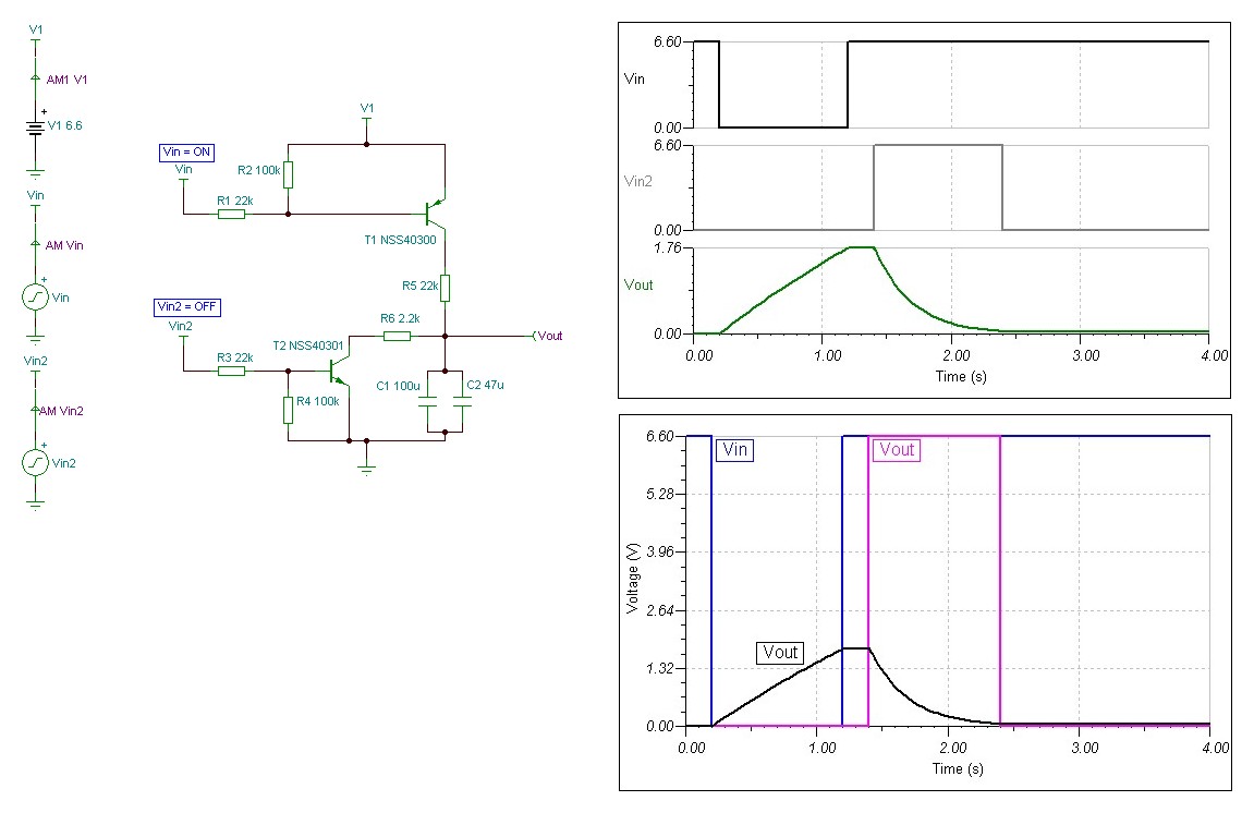
PRECISION CLAMP FOR TORCH WAVESHAPING STUFF V3.JPG


Is there some way of making the rising slope of Vout be an exponential curve, identical to/the same shape as the falling slope? It can't be impossible to make the capacitor rising slope do something other than linear or curved in the wrong direction (I want to make it 'concave' rather than the natural and undesired 'convex' curve), surely? Or is there any other circuit block that can do this using analog design parts?

Thanks.
 

Hi,

a simple task for a microcontroller.
*****

to make it fall:
* simply discharge a capacitor with an R to GND.
Example: If you want a tau of 1s. then use a 1uF capacitor and dicharge it with a 1MOhms resistor.

how does it work?
At fully charged capacitor (let´s say 2.5V) the initial discharge current is 2.5V/1MOhm = 2.5uA
when the capacitor is 2V then the discharge current is 2uA
when the capacitor is 1V then the discharge current is 1uA
and so on.
--> The fall rate is proprotional to the current.

and that´s the key for the rising shape:
--> the rise rate is proportional to the current, too.

for the same shape, but backwards you (just) need to run the current in the opposite manner.
at 1V capacitor voltage you need a charge current of 1uA
at 2V capacitor voltage you need a charge current of 2uA
at 2.5V capacitor voltage you need a charge current of 2.5uA
and so on.
Let´s say you want to use an 1M as charge resistor, too,...
then at 1V capacitor voltage you want 1V across the 1M giving a total of 2V
then at 2V capacitor voltage you want 2V across the 1M giving a total of 4V
then at 2.5V capacitor voltage you want 2.5V across the 1M giving a total of 5V

The solution looks simple: Just use an OPAMP with gain of 2 and connect the "charge" resistor to it´s output.

two problems:
1) you need to stop the charge at a capacitor voltage of VCC/2. So 0V means 0% brightness, VCC/2 means 100% brightness.
2) at zero capacitor voltage ... the charge current will be zero, too (ideally). But this means the capacitor does not charge at all.
--> you need a minimum charge current.
Let´s say you want to use 5s (5 tau) then starting from 2.5V down it gives an end voltage of jsut 17mV. To charge the capacitor you need to ensur that the OPAMP ouput is 2x17mV = 34mV minimum.

Klaus
 
  • Like
Reactions: d123

    d123

    Points: 2
    Helpful Answer Positive Rating
You can make an exponentional ramp generator with rising and falling ramp like below.

1603996021067.png


Another possible solution is a linear ramp gernerator with a succeeding non-linear network, either true exponential function or approximated with piecewise linear transfer characteristic.
 

Attachments

  • exponential ramp.zip
    1.1 KB · Views: 142
  • Like
Reactions: d123

    d123

    Points: 2
    Helpful Answer Positive Rating
Hi,

Thank you. They are both great solutions, especially as there are no BJTs or MOSFETs in either circuit.

Thanks for the clear explanation, Klaus. I wouldn't have understood how the idea works otherwise.

I was trying to think about it last night, and think the solution in post #2 - for a 5V supply - would need the input signal from the pushbutton(s) to be limited by say a TL431 to 2.5V and fed into a non-inverting integrator biased at mid-supply to produce the input signal to the capacitor-charging op amp to get the incremental 1V, 2V, 2.5V signal from a pushbutton pulse of varying duration, wouldn't it?

I could only think of op amp + MOSFET current source and a complementary current sink but there are still transistors in that version, and the current source value is dependent on Vsupply which is inconvenient for a 3.9V to 6.6V supply. I think that part of the circuit needs an LDO to simplify the dedign by limiting Vs to e.g. 3.5V and not have such a 'wide' voltage range affecting both some signal levels and shunt reference supply current variation.

Look forward to working through your solutions over the weekend when chores are done. Many thanks, again.
 

Hi,

I was trying to think about it last night, and think the solution in post #2 - for a 5V supply - would need the input signal from the pushbutton(s) to be limited by say a TL431 to 2.5V and fed into a non-inverting integrator biased at mid-supply to produce the input signal to the capacitor-charging op amp to get the incremental 1V, 2V, 2.5V signal from a pushbutton pulse of varying duration, wouldn't it?
No. to discharge a capacitor you don´t need voltage steps 2.5V, 2.0V, 1.0V ....because the voltage automatically goes down because of the dicharge current.The same (or similar) is with the OPAMP output....it automatically creates the necessary voltage .No steps. Analog.

Btw: both solutions are very similar. See the OPAMP in Gain= +2 configuration.

Klaus
 
  • Like
Reactions: d123

    d123

    Points: 2
    Helpful Answer Positive Rating
Hi Klaus,

Oh, okay, I see now. Thank you. Yes, I see that, too.
 

I am trying to work out the circuit in post#3 does it work the following way:
S2 is on and the opamp ouput is low so initially the voltage on C1 is low.
When S1 is on, there is a small leakage current from D2 and C1 charge a bit and then the opamp will take over. D1 will clamp the voltage of C1 to the voltage divider ratio plus the diode drop.
Is this how it goes?
 

Hi,

Finally got to do my simulating homework (up to a point) this morning, did a few sums Thursday night. Also interested in Tyassin's question.

I got to:

Rdiv top = 2.769V
Rdiv bottom = 461mV
I Rdiv = 923uA

2.769V + 0.461V = 3.23V = Vcapacitor max.

I suspected the reference voltages increase slightly as OA vout rises, which they do by a few mV in the simulation. Not sure if that is intentional or is a quirk of the circuit.

(This next part may be wrong...)

100k * 1uF = 0.1 seconds = ~0.5 seconds to reach Vclamp
1V/100k = 10uA; 3.23V/100k = 32.3uA

I think closing S1 is like a start-up circuit - it sends a voltage pulse into OA IN+ to generate an output voltage (461mV * 2 = 922mV; 922mV/100k = 9.22uA = ~10uA), after this point the feedback is regenerative (correct term?), so it becomes exponential, and the more the capacitor charges, the higher the op amp output becomes until it reaches the clamp level. Closing S2 pulls IN+ to ground so it begins to discharge the capacitor by sinking current and the regenerative feedback makes it become an exponential function.

I guess one of the diodes performs a clamping function in conjunction with the resistive divider but I can't figure that bit out, especially as it seems related to (Vdiv 1 + Vdiv2).

PRECISION CLAMP FOR TORCH WAVESHAPING STUFF V4A.JPG
 

Hi,

VF4IN+ signal has two switches.

If both switches are OPEN, then the node is floating. Voltage is unpredictable, function is unpredictable then. Avoid floating nodes.

Klaus
 
  • Like
Reactions: d123

    d123

    Points: 2
    Helpful Answer Positive Rating
Hi,

Hope it's okay to slip a question related to the circuit into this thread, if not per se related to the original question in this thread - it's to avoid several threads about one little circuit.

I just wanted to check, a very, very elementary question: When Vbatt is 6.6V, where will the spare 2.7V go - across the NMOS drain-source or across the 3R3 resistors?

I assume across the NMOS as the OA is controlling the current at 60mA via the 720mV ref and 12R sense resistor.

_20201031_155805.JPG
 

Hi,

you have (known):
(from top = 6.6V)
6.6V, 0.066V across R3, 3V across LED

(from bottom = 0V):
0V, 0.72V across Shunt.

The only unknown is the voltage across the MOSFET. And thats how it should be . The MOSFET is the current regulating device. It adjusts its voltage (according available voltage) to maintain costant current.

The given R_DS_ON is not valid in this case. This is for switching "hard ON" only = saturated.

You are in regulating mode. Thus the voltage across the MOSFET is 2.814V @ 0.06A which gives a MOSFET R_DS of 46.9 Ohms.

Klaus
 
  • Like
Reactions: d123

    d123

    Points: 2
    Helpful Answer Positive Rating
Hi Klaus,

Thank you very much. Never knew difference between switching and regulating on resistance, interesting.
 

Hi,

Factoring suggested super exponential circuit into existing torch circuit, the attached drawing is what I understand might work. Are there any issues with placing the clamps in the feedback loops of U1 and U3?

If any of it is comprehensible, do the formulas look right, I feel like dV = (i In/dt)/C might be a nonsense approach to calculate volts per second at C1 node, hopefully not.

Bizarre sudden metamorphosis of 4.998 seconds into 4.844 seconds halfway through calculations is a mistake, sorry about that, various bits of paper and calculations made me put the wrong time from a calculation yesterday and as it is a 'trivial' difference, I'd rather not re-do the whole thing...

If needed to know, C1 node also goes into two voltage followers and an NMOS drain, basically - that section works.

_20201101_132732.JPG
 

Hi,

Just realizing...it's exponential, not linear... Exponential capacitor charging curve circuit is 1*2 > 2^2 > 4^2, etc...

If RC decay time to x% of original value is: - tau * (natural logarithm of % of original value),

e.g.
t = - 0.001 seconds * (natural logarithm of 50%)
t = 0.000693 seconds

can the minus sign be removed, and % be replaced with e.g 500% (5 tau) to estimate exponential RC curve to 99% charged?

i.e. t = 0.001 seconds * (natural logarithm of 5)
t = 0.001609 seconds
--- Updated ---

Hi,

Was working out/trying to work out, from decay formula:

t discharging = - tau ln %
(percent is written as e.g. 0.01 to 0.99)
t charging = tau ln %
(percent is written as e.g. 1 to 100)

So, a tau of 6k8 * 294uF = 0.996 seconds
and a tau of 470R * 294uF = 0.138 seconds

Charge to 100% and discharge to 1% = 4.586 seconds for tau of 0.996 seconds.

Charge to 100% and discharge to 1% = 0.635 seconds for tau of 0.138 seconds.

Is this method correct now? I noticed that using 99 as charging percent value is only 4.576 seconds, I'd have expected it to match discharged to 1% value, so not sure how valid or accurate charging calculations may be.
 
Last edited:

Status
Not open for further replies.

Part and Inventory Search

Welcome to EDABoard.com

Sponsor

Back
Top