Continue to Site

Welcome to EDAboard.com

Welcome to our site! EDAboard.com is an international Electronics Discussion Forum focused on EDA software, circuits, schematics, books, theory, papers, asic, pld, 8051, DSP, Network, RF, Analog Design, PCB, Service Manuals... and a whole lot more! To participate you need to register. Registration is free. Click here to register now.

"Virtual ground" quarterwave stub for varactor in microstrip VCO.

Status
Not open for further replies.

Terminator3

Advanced Member level 3
Joined
Feb 25, 2012
Messages
802
Helped
71
Reputation
142
Reaction score
63
Trophy points
1,308
Activity points
9,027
Article:
https://www.adv-radio-sci.net/4/21/2006/ars-4-21-2006.pdf
Frequency tuning is realized by adding varactor loading to matching circuit line. As i understand it works as varactor loaded line phase shifter. I can't understand meaning of this phrase:
In both designs
the varactor diode is connected to a virtual ground provided
by a λ/4 transformation in order to keep the biasing effort
moderate.

As i understand λ/4 stub works as narrow-band short-circuit for varactor at RF. What is the meaning of "keep the biasing effort moderate"?

Also, in some designs there is no any RF grounding at all! For example:
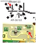
vco.jpg
1) upper image represents VCO from article ars-4-21-2006.pdf with quarterwave "virtual ground" stub.
2) lower image represents another VCO, where varactor does not have any "virtual ground" quarterwave stub, only DC biasing.

I tried to use smith chart and can't understand how the second schematic is working, because series capacitance (varactor) can't transform open-circuited impedance (Г=1, a=0 deg) on smith chart, and parallel capacitance to ground is required. So adding quarterwave makes sense (Г=1, phi = 180deg) and impedance can be transformed using varactor capacitance to some point for frequency tuning.
 

It appears that one side of the varactor bias is used to bias the active gain device which avoids capacitor blocks thus avoiding additional parasitics.
 
A varactor should see a DC voltage between its contacts.This lambda over 4 layout might be layed on for harmonics.
 
Re: "Virtual ground" quarterwave stub for varactor in microstrip VCO.

What about second image (color photo)? Open-circuited stub with varactor at open end.
If i put open-circuited impedance point on Smith chart and add series capacitor (varactor with some DC biasing), impedance would not be altered! 0.01pF or 1000pF, results are the same. So i wonder how it performs frequency tuning? Although there a little solder on open end of varactor, which can perform as a little stub.

- - - Updated - - -

I have additional question. Why sometimes matching stubs made non-50 Ohms? Usually all examples use 50-ohm matching stubs (open, short). Sometimes quarterwave transforming, which is easy to understand.
But why one would use something like 20 Ohm wide open-circuited stub on a 50 Ohm line? Also i have seen high impedance matching stubs (something like 100-200 Ohm stub attached to 50-Ohm line). Why not staying with 50-Ohm open stubs?

My guesses are:
1) Maybe it is coming from design approach? Lumped element circuit -> distributed elements microstrip circuit. But is is more related to filters i think.
2) Somehow using non-50 Ohm matching stubs can reduce size of matching network?
3) Somehow using non-50 Ohm matching stubs can influence bandwidth of matching circuit? (Long time ago i read that thin quarterwave stubs / resonators have wider bandwidth).
 

Re: "Virtual ground" quarterwave stub for varactor in microstrip VCO.

Choice of high and low impedance depends upon design requirement.
If you need capacitive matching,you will go for low impedance which are broader and more capacitive.
While narrower and inductive stubs are used in other cases.

As far as virtual ground is concerned,its only RF ground and acts as open circuit for dc,hence simplifies biasing.
 
Unfortunately, i do not have this pcb anymore. Too much solder can indicate via on the right side of varactor, but DC biasing looks impossible to achieve this way. But it was two-layer PCB, innel layer may have answers.
If solder dot is treated like lambda/8...lambda/16, there are small phase tuning still using varactor.

There is one question bothering me for a long time:
vcovco.jpg
Many designs with DC-block (marked "1" on this image) have wide area right before dc-block thin coupled lines. Many microstrip band-pass filters made this way too: there is pretty wide area placed right before filter and after filter. I read some books, did some calculations. There is odd impedance, even impedance, coupled lines analysis and similar stuff. But it is all about filter or coupler itself. None of books i read consider this quarter-wave(?) area right before coupled part starts. So what is this thing? It looks like quarter-wave transformer. It is very wide, so it looks that they try to achieve very low impedance, but why?
I have two theories:
1) calculated line width for Z0=50 Ohm are too thin, or not optimal, so they use some 20 Ohm, etc..
So all coupled elements will have different width. But here it is unclear how they decide wich Z0 is good for filter input and output.
2) some other reason i do not know yet.

Another thing is marked "2" on image. It is half-wave resonator in microstrip parallel feedback oscillator. Interesting thing is that it is connected to phasing line. What is the purpose of such connection?
1) To obtain lower Q-factor? (to obtain wider frequency tuning using varactor)
2) To add more power into feedback?
 
Last edited:

Thank for your answers!
Is it conditionally stable transistor in parallel feedback oscillator?
It is difficult to make this transistor stable+have good gain, so maybe move it most unstable frequency to parallel feedback center frequency area using source stub/phasing line. And after startup it somehow will be "pulled" to frequency of parallel feedback resonator? Worst thing if two frequencies of oscillation would exist/spontaneously switching.


still have two doubts:
1) wide part before microstrip DC-block. Why it is made so wide (low impedance)?
2) why half-wave resonator is connected to phasing line?
 

I have additional statements to clarify my understanding of varactor frequency tuning.

Most frequently used configurations:

1. Short-circuited microstrip stub with varactor.
Short-circuited stub forms inductance L, varactor provides tunable capacitance C.
Then we can obtain resonator frequency using formula F=1/(2*Pi*Sqrt(L*C))
Looks like pretty easy to design.

2. Microstrip line loaded with varactors (parallel connection).
Phase shift through microstrip line depends on signal frequency and it's length. Dividing microstrip line to finite elements of some size allows us to represented each element by it's capacitance and inductance. Loading line with varactors (tunable capacitances) allows us to have tunable phase shift through microstrip line "pieces".
Parallel and series connection of varactors to microstrip lines:

3. Microstrip line or other structure magnetically coupled to microstrip stub with varactor element. For example, it can be dielectric resonator or hairpin resonator coupled to small varactor-loaded microstrip element.
For example:

The coupling mechanism of AR is shown in Fig. 2. Capacitive variation in the MESFET varactor has been transformed into inductive variation at the plane of coupling.
Figure 2 shows that coupled shorted varactor + line gives additional variable inductance coupled to resonator.

Confusing parts in method N3: how to calculate final inductance (influence of coupled varactor line) to estimate frequency tuning range? Where i can find such formulas. I was hoping to find complete example with calculations (coupling, distance between resonator and line, etc..)
 

Can someone comment on how is biasing done for varactor on this image?
broken link removed
The problem is: i suspect that varactor is grounded with VIA to gnd (red arrow)
But also there is thin biasing line provided to this point, which is looks pretty strange.
Simulation of similar schematic showed, that there must be RF ground at that point to provide good performance. It can be made using VIA to GND or quarterwave open-circuited stub. It is obvious, that point on the right sight of varactor is far form quarterwave, and can give only some capacitive impedance, which does not provide any acceptable tuning performance. The only option left is VIA to GND, but then varactor biasing is somehow tricky.
I can imagine:
1) VIA have some resistance, say 0.000001 Ohm. Then one biasing resistor can be used to form resistive voltage divider. But in this case voltage divider must be driven with huge voltage, maybe like 100 or 1000 volts (i did not do any calculations, but idea is that most voltage drop occurs through normal chip resistor, and only small amount is available before VIA to GND voltage drop). VIA certainly have some resistance, but it looks unrealistic.

2) There are hidden ground plane, which is biased through resistors somewhare. It is three copper layer PCB (two dielectric layers). So on a hidden plane, there can be some ground plane which is biased through resistor?
Please comment

3) Transistor is biased relative to ground in a such way, that transistor biasing remains constant (VGs, Vds, etc.), but transistors drain biasing is tunable relative to ground. In a such way transistor biasing is constant, but the whole transistor voltages can be altered like Vd+V1, Vg+V1, Vs+V1, so additional V1 voltage is achieved between drain and ground. Looks feasible, but complicated to me.
 
Last edited by a moderator:

Can someone comment on how is biasing done for varactor on this image?

For prototyping (one or two pcbs) I have inserted small chip capacitors vertically thru drilled holes in a .06" thick substrate and soldered top and ground for low inductance AC ground!
 
Interesting method, thank for your comment!
 

Status
Not open for further replies.

Part and Inventory Search

Welcome to EDABoard.com

Sponsor

Back
Top