Continue to Site

Welcome to EDAboard.com

Welcome to our site! EDAboard.com is an international Electronics Discussion Forum focused on EDA software, circuits, schematics, books, theory, papers, asic, pld, 8051, DSP, Network, RF, Analog Design, PCB, Service Manuals... and a whole lot more! To participate you need to register. Registration is free. Click here to register now.

Vin CM in differential amplifier

Status
Not open for further replies.

giri_lp

Member level 3
Member level 3
Joined
Feb 11, 2006
Messages
61
Helped
0
Reputation
0
Reaction score
0
Trophy points
1,286
Activity points
1,657
vin cm

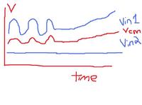
The concept of input CM in differential amplifier is unclear. Is this CM is DC CM or AC CM? When we apply an ac signal to the diffrential amplifier What is the CM voltage? Is this the offset from 0 or do we have to look this with refrerence to differential signal ? Please explain the Vin CM concept in differential amplifier
 

differential amplifiers by razavi

giri_lp said:
The concept of input CM in differential amplifier is unclear. Is this CM is DC CM or AC CM? When we apply an ac signal to the diffrential amplifier What is the CM voltage? Is this the offset from 0 or do we have to look this with refrerence to differential signal ? Please explain the Vin CM concept in differential amplifier

It´s quite simple:

Vcm is defined as follows: Vcm=(Vin1+Vin2)/2
That means, Vcm is the arithmetic mean of both input voltages (even if one input is zero or negative).
The background is as follows: Each differential voltage can be split in two parts:
(Vin1+Vin2)/2=Vcm and (Vin1-Vin2)/2=Vdiff/2

This results in Vin1=Vcm+Vdiff/2 and Vin2=Vcm-Vdiff/2.

You see, there is a common part for both voltages. Exception: Vin1=-Vin2.

Was this your quesstion ?
 

    giri_lp

    Points: 2
    Helpful Answer Positive Rating
input swing differential amplifier

by definition, VCM=(Vin1+Vin2)/2 (no exceptions)


    giri_lp

    Points: 2
    Helpful Answer Positive Rating
differential signal change offset

HI EECS4ever and Lvw,
Thanks for you replies. You answered my question.


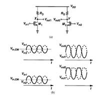
The above image is cut from Razavi Text. Where there are two differenital input signal. One with higher Vcm and the other with lower Vcm. How this is obtained, Do we have to reduce the signal swing? When I actually want to change the Vswing what should be done?

Please help me here
 

simple differential amplifier

giri_lp said:
HI EECS4ever and Lvw,
Thanks for you replies. You answered my question.
The above image is cut from Razavi Text. Where there are two differenital input signal. One with higher Vcm and the other with lower Vcm. How this is obtained, Do we have to reduce the signal swing? When I actually want to change the Vswing what should be done?
Please help me here

I am a bit confused about the output voltages as I don´t know why clipping appears for the second case with lower input voltages. Perhaps both output diagrams are interchanged ?
 

differential amplifier operating point cmos

The two signals are generated with different common mode voltages by the circuitry that produced them. For now assume that the are produce by a signal generator.

When you say Vswing, I assume that you are referring to the output swing of the circuit. If we assume that the circuit is linear, We can approximate the output swing as follows. Vout = A*vin. where A = gm * (Rout || Rd) where gm is the transconductance of the transistor, and Rout is the output impedance. The output swing amplitude is the product of the input swing , the transconductance, and the effective output impedance of the circuit. You can change any of the variables listed to change vswing.


Clipping occurred on the 2nd input signal with lower common mode. This is because the common-source amplifier is an inverting structure. Lower input common mode voltage will produce a higher output common mode voltage as shown in the diagram.

you can check with KCL as well. as the input common mode voltage decreases. The current through the transistor, IDS, decreases since IDS is approx 1/2 W/L u COX (Vgs-Vt)^2. Now the output voltage is Vout = VDD-IDS*RD. As IDS decreases, Vout goes up.
 

    giri_lp

    Points: 2
    Helpful Answer Positive Rating
eecs4ever said:
..............
..............

Clipping occurred on the 2nd input signal with lower common mode. This is because the common-source amplifier is an inverting structure. Lower input common mode voltage will produce a higher output common mode voltage as shown in the diagram.

OK, I got it. Thanks. This may be the reason. But it is very uncommon that the common mode part of the input voltages determine the operating point of the transistors. This has confused me a bit.
Normally, coupling capacitors are to be used.

Added after 10 minutes:

Ohh, I am afraid I´ve made an error.
As this discussion has started under the keyword "differential amplifier" I was of the opinion that the last question (concerning Razavi´s circuit) was related also to a differential amplifier. (That means, I did not look at the diagram carefully).
Only now I have discovered that both stages have no connection at all. It is no differential amp.
Therefore, forget my comments. Sorry.
 

Yes. The annoying point with the shown figure from "Design of Analog CMOS Integrated Circuits" is, that it was obviously posted without thinking respectively reading the few lines of text below.

The circuit designated "Simple differential circuit" rather than differential amplifier is only used by Razavi to motivate the introduction of the differential pair. So the text, that explains very detailed the reason for signal clipping in the above circuit ends: "A simple modification can resolve the above issue".

I'm helpless with this kind of text book use.
 

"Clipping occurred on the 2nd input signal with lower common mode. This is because the common-source amplifier is an inverting structure. Lower input common mode voltage will produce a higher output common mode voltage as shown in the diagram."

Hi EECS4ever thanks for that note!! :)
Though I can understand this clipped behavior in large signal analysis, how this
explains if we do small signal analysis? If I correct, considering amplifiers operate in saturation region and clipping are looking contradictory..
 

Hi,

Yes giri_lp you are correct. When clipping occurs, the circuit is no longer linear. We cannot approximate the output to be Vout = A * vin in this case. So when clipping occurs, you can use large signal analysis to calculate the output voltage.
 

    giri_lp

    Points: 2
    Helpful Answer Positive Rating
Status
Not open for further replies.

Part and Inventory Search

Welcome to EDABoard.com

Sponsor

Back
Top