mtwieg
Advanced Member level 6

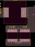
I usually have my layouts done by a third party, and they generally insist that no vias ever be placed underneath large capacitors and inductors (not referring to via in pad). See below: the pink shaded areas are via keepouts.
I can understand this caution in a couple situations, like if it's an inductor with a conductive body (very rarely the case) or if the vias reduce creepage/clearance near high voltage nodes. And this would only apply to cases where the vias are exposed through the soldermask. But the layout people are pretty adamant on enforcing these rules, regardless of whether the vias are tented or what the component is or how its used. Are there any manufacturing pitfalls I'm not aware of, or is this just pure superstition?

I can understand this caution in a couple situations, like if it's an inductor with a conductive body (very rarely the case) or if the vias reduce creepage/clearance near high voltage nodes. And this would only apply to cases where the vias are exposed through the soldermask. But the layout people are pretty adamant on enforcing these rules, regardless of whether the vias are tented or what the component is or how its used. Are there any manufacturing pitfalls I'm not aware of, or is this just pure superstition?


