Rajinder1268
Full Member level 3

Hi all,
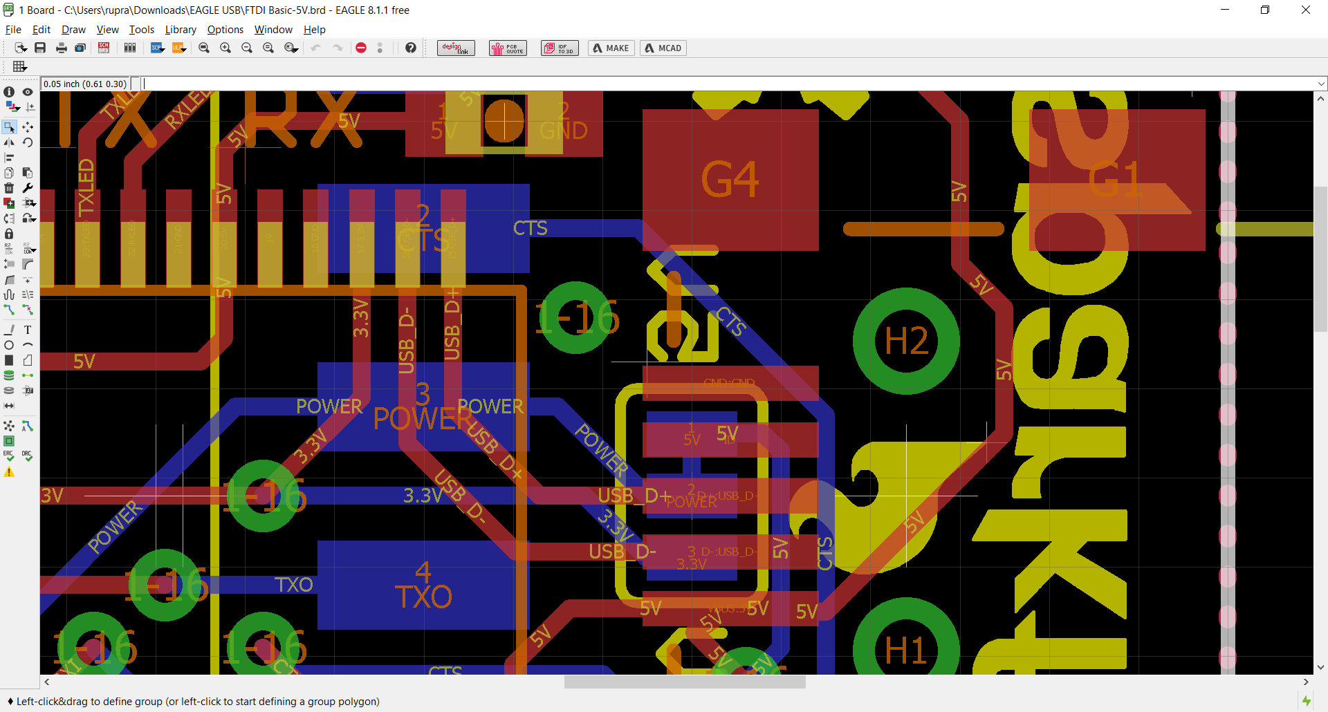
I have attached a copy of a board which has USB tracking of D+ and D- signals from a USB connector. I am going to do something similar. Looking at the layout design in the picture, Is there going to be an issue with tracking the D+/D- lines as shown in terms of getting the same length? Or is it best to turn the microcontroller by 90 degree clockwise and then adjust its position to get the length same?
My second question is that I am going to connect the shield of the connector to GND via a 0R resistor. Do I connect all the shield pins on the USB connector with a thick track 2.54mm or similar and then to the 0R and then the 0R connected to the main GND.
I was thinking of having a solid GND on the BOTTOM layer, the Top layer being signal tracks, tracks for VCC. Is it a good idea to have a polygon plane for the VCC or will tracks be sufficient.
Lastly, i was thinking of having additional GND on the remaining of the Top PCB - which will be stitched to the BOTTOM layer GND through VIAS.
Does my approach seem ok?
Thanks in advance


