TokTok12
Junior Member level 2

Hi all,
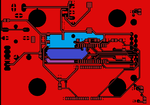
I’m aware this must be a well covered topic on forums but having read a lot of links I seem to be stuck. Essentially I've got my brd file which I routed using a combination of manual routing and using the auto-router. I have a couple of remaining airwires and I’m wondering the best way to get rid of them/complete the connections joined by an airwire.
Here are the sch and brd files: View attachment SCH AND BRD.zip
NOTE: Since I have defined a "GND" polygon on both the top and the bottom layer over the whole board, the traces called "GND" are not routed, as it is already connected when loading the GND polygons but it is on some of the GND pins that I have remaining airwires.
Any suggestions are appreciated.
Regards,
TokTok.
Last edited:

