yefj
Advanced Member level 5

Hello ,i have a general problem in many of my components where i cant route to the center of the PAD.
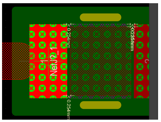
In my PCB component R1 i try to route to the center and it stop right before the center as shown bellow.
on explanantion i think they made the keepouts too wide.
but i totally could not select the keepout shape of the component.
i dont know if its the keepout issue.
What could be causing this?
My project is shown in the attached link.
Thanks.
https://drive.google.com/file/d/1Mt12pudndDqQICTlWCRv3BfZk3TGiY2F/view?usp=sharing
Last edited: