Welcome to our site! EDAboard.com is an international Electronics Discussion Forum focused on EDA software, circuits, schematics, books, theory, papers, asic, pld, 8051, DSP, Network, RF, Analog Design, PCB, Service Manuals... and a whole lot more! To participate you need to register. Registration is free. Click here to register now.
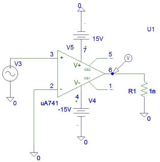
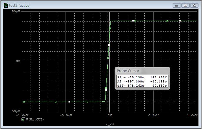
hi, i meet a question when i do this simulation.
i use following test circuit to analyse the offset voltage of us741. But the result is strang. Output equals to 0 when input is 0.19uv. But in its datasheet, this voltage should be 5mv.
Could you point my mistake, please?
Thanks!
Read the datasheet more thoroughly! I surely doesn't say, the offset voltage should be 5mv. It may be up to +5mV or -5mV, typically it's less. Simulation models may assume any arbitary value, some have a considerable offset, others don't.
Thanks for your reply. In the datasheet, it mentions MAX offset voltage is 5mv and TYP is 1mv. So the limitation is +/-5mv and the different test circuits get different offset voltage results. Could anybody provide the other test circuits please?
I don't understand which test cicrcuits you're refering to. Many OP model have a VOS model parameter, that can be overriden in the device instantiation to operate the circuit at different OP offset voltages.
This site uses cookies to help personalise content, tailor your experience and to keep you logged in if you register.
By continuing to use this site, you are consenting to our use of cookies.