bywarfare
Newbie level 3

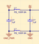
I'm designing a PCB that has no earth ground but there are lots of connectors with shielding pins such as USB, Ethernet, and HDMI also their TVS diode to protect from ESD. This PCB has to pass the EMC tests, especially the immunity test, with success. I used a CMC filter in the input supply of the circuit, there are no Y capacities because there is no earth ground or housing shield. You can see the input filter and the output of the DC-DC converter filter circuit in the following image.


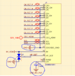
Where should I connect the shields of the connectors and the GND pins of the TVS for this circuit? In a few articles it is said that it should be connected to ground with 100nF, but I could not decide which gnd to connect. Do I really need 100nF, I'm not sure of that either. For example, in the picture below, it makes more sense to connect to unfiltered GND with 100nF otherwise all noise will flow to the filtered GND, am I wrong? But I have no idea for the chassis pins and TVS on HDMI. If I connect it to the unfiltered gnd, can the noise outside the device disrupt the communication?


Finally, if there is a source where I can learn such details, I would be very glad if you could suggest to me.
Thanks.


Where should I connect the shields of the connectors and the GND pins of the TVS for this circuit? In a few articles it is said that it should be connected to ground with 100nF, but I could not decide which gnd to connect. Do I really need 100nF, I'm not sure of that either. For example, in the picture below, it makes more sense to connect to unfiltered GND with 100nF otherwise all noise will flow to the filtered GND, am I wrong? But I have no idea for the chassis pins and TVS on HDMI. If I connect it to the unfiltered gnd, can the noise outside the device disrupt the communication?


Finally, if there is a source where I can learn such details, I would be very glad if you could suggest to me.
Thanks.