Continue to Site

Welcome to EDAboard.com

Welcome to our site! EDAboard.com is an international Electronics Discussion Forum focused on EDA software, circuits, schematics, books, theory, papers, asic, pld, 8051, DSP, Network, RF, Analog Design, PCB, Service Manuals... and a whole lot more! To participate you need to register. Registration is free. Click here to register now.

[SOLVED] Trouble with frying 74LS11N AND Gate

Status
Not open for further replies.

areddon

Newbie level 4
Newbie level 4
Joined
Jan 12, 2020
Messages
6
Helped
0
Reputation
0
Reaction score
0
Trophy points
1
Activity points
91
In a prototype board for Lithium battery charge control, I have a three input AND gate (74LS11N).

The inputs to the AND gate are:

1A = 5/0 volts from a digital output pin on an Arduino nano
1B = drain of an N-channel MOSFET (HUF76423P3) acting as low side switch on a 5 volt supply
1C = drain of a P=channel MOSFET (STP10P6F6) acting as a high side switch on a 5 volt supply

The output from AND gate (1Y) goes to the gate of another N-channel MOSFET (HUF76423P3) which acts as a low side switch on the 12 volt control signal to a solid state relay.

In testing the prototype, the gate is not working as expected. Upon removal and testing (tried twice) I found the AND gates had one input pin that did not affect the state of the output

I did not take great care against ESD so it is possible that i damaged the AND gate during assembly, BUT before trying a third time with proper ESD protection, I would like to know:

a) Is there something obvious in this circuit that could be frying the AND gate?
b) Is the LS gate appropriate or would a HC gate be better?
 

Your description is partly unclear. Is there anything else connected to inputs 1B and 1C except the transistor drain terminals? If so, 1C will surely receive permanent high signal and not work as expected.

I'd appreciate a schematic.

ESD isn't a big problem with ancient 74LS series, more likely input overvoltage. A design rule says inputs shouldn't be connected to VCC directly, only through series resistor to increase the overvoltage immunity. In so far driving 1C to VCC by low ohmic PMOS switch isn't optimal, apart from the missing pull-down resistor.
 
There is nothing else attached to 1B or 1C except the transistor drain terminals.

Would it be acceptable to post a PDF of a hand drawn schematic or is that a bit rude/disrespectful?
 

Hi,

"Connected drain" to an input... also need pullup / pulldown resistors.

General rule: Don't leave any input (used or not) of any IC floating. With "LS" type they may be pulled low internally.
But "LS" types are old, slow, power consuming and provide low HIGH levels. I'd use HC or HCT types. (Mainly differ on supply voltage range and input HIGH levels)
But there are a lot of other families with different features.

*******
Your application seems to use high switching currents. Thus you need a proper PCB layout. No breadboard!
You need a true power plane. Copper pour is no GND plane!

Also each power supply input of each IC should have it's own decoupling capacitor.
Use a (free) schematic software with PCB layout feature.

********
Would it be acceptable to post a PDF of a hand drawn schematic or is that a bit rude/disrespectful?
Many times here in this forum I already recommended this.
Any schematic - even hand drawn - is better than none. There's nothing against hand drawn ones.
No PCB layout without schematic
But as soon as you want to do a PCB layout I recommend to use software.

Klaus
 
Would it be acceptable to post a PDF of a hand drawn schematic or is that a bit rude/disrespectful?
Any kind of readable and meaningful documentation is welcome.

General rule: Don't leave any input (used or not) of any IC floating. With "LS" type they may be pulled low internally.
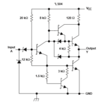
LS has input diodes and must be pulled down actively. Floating input is recognized as high but should be pulled up to at least 2.4V for better noise margin.

74ls.PNG
 
The 74LS11 IC is a triple, 3 input AND gate.

What are you doing with the inputs of the two other unused gates?
 
I'd start with simple testing of those "bad" logic ICs
and see whether the inputs all show same IIH, IIL or
some are "out of family" and thus suspect for damage.
Given that you seem to be playing with coils it seems
likely to me that EOS (electrical overstress) is more
likely than handling ESD. If you have two bad and they
both have the same failure signature, same pin(s), that
ought to point you at the source of the problem.

It's also be worthwhile to put 'scope probes to the empty
socket (or where the ill part is removed, from) and look for
overshoots / sustained overvoltage on inputs and outputs
as you mess with the control signals' sources. 5VDC plus
inductor plus switching equals "something other than 5VDC".
So don't assume that what you say it is, is what it is.
 

FmV, KlausST, schnidtt trigger, and dick_freebird:

All great and helpful responses. Added resistors, tied down the pins on unused gates, and good success on my third try.

Thank you all.
 

Status
Not open for further replies.

Part and Inventory Search

Welcome to EDABoard.com

Sponsor

Back
Top