Continue to Site

Welcome to EDAboard.com

Welcome to our site! EDAboard.com is an international Electronics Discussion Forum focused on EDA software, circuits, schematics, books, theory, papers, asic, pld, 8051, DSP, Network, RF, Analog Design, PCB, Service Manuals... and a whole lot more! To participate you need to register. Registration is free. Click here to register now.

Trouble understanding the FP5139BWR-LF pin 4

Status
Not open for further replies.

sulfur101

Newbie level 6
Newbie level 6
Joined
Jul 20, 2022
Messages
13
Helped
0
Reputation
0
Reaction score
0
Trophy points
1
Activity points
77
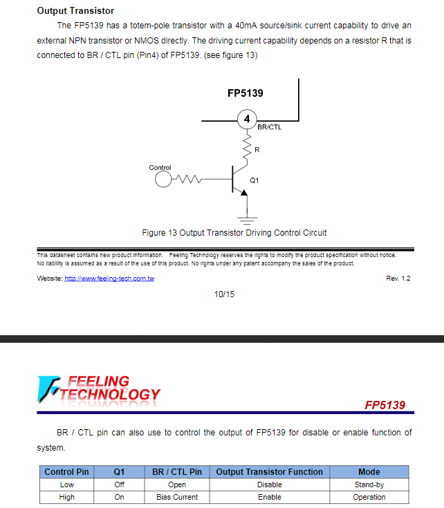
hello every one i am trying to understand the BR/CTL pin on the FP5139BWR-LF IC for a buck boost converter.
so what i am confused about is the control where is it coming from and will i be able to get it
1694024678826.png


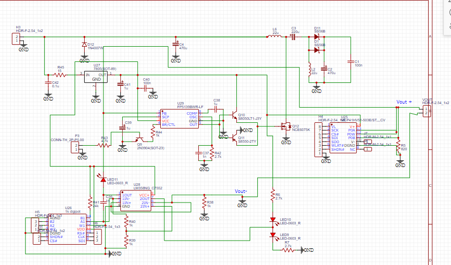
also my design is below if you find any issues that i cant catch, the inductors L6, L2 are supposed to be iron core but this is what i can find at the moment.
1694024750624.png
 

as you can see from the examples on the datasheet, you can implement an ON/OFF switch with an external transistor on the pin 4.
you can omit that external control, just by placing a Resistor (390 ohm) from pin 4 to GND. (always ON)
 

Your schematic looks broken, particularly the Vout and FB path. Consider that a boost converter without operational feedback can easily destroy the switcher transistor.
 

Status
Not open for further replies.

Similar threads

Part and Inventory Search

Welcome to EDABoard.com

Sponsor

Back
Top