raghurocks
Member level 1

- Joined
- Jul 3, 2012
- Messages
- 33
- Helped
- 2
- Reputation
- 4
- Reaction score
- 0
- Trophy points
- 1,286
- Location
- India,Gujarat
- Activity points
- 1,568
Hai every one,
I have been working under varying the brightness of the ac loads using the triac and a microcontroller.
I have written code for it and I tried for the output on the simulator as we cannot see the dimming on the simulator I have seen the output voltage which is varying for different levels but practically I am not getting the output which I am getting on the simulator
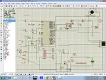
Here is the schematics I have done......

and the code I have written is........
Concept:
The concept I have used is that if I want a less brightness the I will increase the delay time for the triac to trigger where we are increasing the delay angle and decrease the conduction there by decreasing the rms output so like wise I for example if I want 20% brightness I will give zero pulse for 8 ms and will give high pulse for 100us(0.1 ms) and then off for the remaining time like wise I have divided into 16 levels where the input I give from the switches(based on the basic concept of the TRIAC) which you can see on the above code
Problems:
The problems I am facing in the hardware are the
1.In the schematic I am grounding the ac neutral and the T1 of the triac to the circuit ground so if I do that on the bread board the lamp is lighting at only one level and the 220 ohm resistor is burning
2.If I don't do the grounding like that the lamp is not at lighting on
I am unable to know where the problem persist
1.whether am I going wrong in detecting zero or
2.producing pwm which indeed depend on the zero crossing
Queries:
1. I don't have the CRO so how to check whether my zerocrossing detector is producing the zero crossing or not
2. And how to check whether my microcontroller is producing the desired pwm wave or not
Any help is very much valuable for me.......
Thanks in advance
I have been working under varying the brightness of the ac loads using the triac and a microcontroller.
I have written code for it and I tried for the output on the simulator as we cannot see the dimming on the simulator I have seen the output voltage which is varying for different levels but practically I am not getting the output which I am getting on the simulator
Here is the schematics I have done......

and the code I have written is........
Code:
 org 00h
 MOV P2,#00H
 MOV P1,#00H
 MOV TMOD,#01H
 MOV SCON,#50H
 MAIN:
 	MOV A,P1;// to take data from the switches into the accumulator
LOOP1:
CJNE A,#01H,LOOP2
	S1:JNB P2.1,S1
SETB P2.0
MOV TL0,#0A4H//0.1MSEC  ON
MOV TH0,#0FFH
CALL DELAY
CLR P2.0
MOV TL0,#3DH//9.1MSEC  OFF
MOV TH0,#0DFH
CALL DELAY
LJMP MAIN


LOOP2:
CJNE A,#02H,LOOP3
	S2:JNB P2.1,S2
CLR P2.0
MOV TL0,#07BH//0.7mSEC	 OFF to set delay angle for 0.7msec
MOV TH0,#0FDH
CALL DELAY
SETB P2.0
MOV TL0,#0A4H//0.1MSEC ON trigger for 100us
MOV TH0,#0FFH
CALL DELAY
CLR P2.0
MOV TL0,#0E1H//9.2MSEC OFF
MOV TH0,#0DEH
CALL DELAY
LJMP MAIN

LOOP3:
CJNE A,#03H,LOOP4
	S3:JNB P2.1,S3
CLR P2.0
MOV TL0,#0F6H//1.4MSEC	 OFF to set delay angle for 1.4msec
MOV TH0,#0FAH
CALL DELAY
SETB P2.0
MOV TL0,#0A4H//0.1MSEC ON trigger for 100us and so on
MOV TH0,#0FFH
CALL DELAY
CLR P2.0
MOV TL0,#066H//8.5MSEC OFF
MOV TH0,#0E1H
CALL DELAY
LJMP MAIN

LOOP4:
CJNE A,#04H,LOOP5
	S4:JNB P2.1,S4
CLR P2.0
MOV TL0,#71H//2.1MSEC	 OFF
MOV TH0,#0F8H
CALL DELAY
SETB P2.0
MOV TL0,#0A4H//0.1MSEC ON
MOV TH0,#0FFH
CALL DELAY
CLR P2.0
MOV TL0,#0ECH//7.8MSEC OFF
MOV TH0,#0E3H
CALL DELAY
LJMP MAIN

LOOP5:
CJNE A,#05H,LOOP6
	S5:JNB P2.1,S5
CLR P2.0
MOV TL0,#0ECH//2.8MSEC	 OFF
MOV TH0,#0F5H
CALL DELAY
SETB P2.0
MOV TL0,#0A4H//0.1MSEC ON
MOV TH0,#0FFH
CALL DELAY
CLR P2.0
MOV TL0,#71H//7.1MSEC OFF
MOV TH0,#0E6H
CALL DELAY
LJMP MAIN


LOOP6:
CJNE A,#06H,LOOP7
	S6:JNB P2.1,S6
CLR P2.0
MOV TL0,#66H//3.5MSEC	 OFF
MOV TH0,#0F3H
CALL DELAY
SETB P2.0
MOV TL0,#0A4H//0.1MSEC ON
MOV TH0,#0FFH
CALL DELAY
CLR P2.0
MOV TL0,#0F6H//6.4MSEC OFF
MOV TH0,#0E8H
CALL DELAY
LJMP MAIN

LOOP7:
CJNE A,#07H,LOOP8
	S7:JNB P2.1,S7
CLR P2.0
MOV TL0,#0E1H//4.2MSEC	 OFF
MOV TH0,#0F0H
CALL DELAY
SETB P2.0
MOV TL0,#0A4H//0.1MSEC ON
MOV TH0,#0FFH
CALL DELAY
CLR P2.0
MOV TL0,#7BH//5.7MSEC OFF
MOV TH0,#0EBH
CALL DELAY
LJMP MAIN

LOOP8:
CJNE A,#08H,LOOP9
	S8:JNB P2.1,S8
CLR P2.0
MOV TL0,#5CH//4.9MSEC	 OFF
MOV TH0,#0EEH
CALL DELAY
SETB P2.0
MOV TL0,#0A4H//0.1MSEC ON
MOV TH0,#0FFH
CALL DELAY
CLR P2.0
MOV TL0,#00H//5.0MSEC OFF
MOV TH0,#0EEH
CALL DELAY
LJMP MAIN

LOOP9:
CJNE A,#09H,LOOP10
	S9:JNB P2.1,S9
CLR P2.0
MOV TL0,#7BH//5.7MSEC	 OFF
MOV TH0,#0EBH
CALL DELAY
SETB P2.0
MOV TL0,#0A4H//0.1MSEC ON
MOV TH0,#0FFH
CALL DELAY
CLR P2.0
MOV TL0,#0E1H//4.2MSEC OFF
MOV TH0,#0F0H
CALL DELAY
LJMP MAIN

LOOP10:
CJNE A,#0AH,LOOP11
	S10:JNB P2.1,S10
CLR P2.0
MOV TL0,#0F6H//6.4MSEC	 OFF
MOV TH0,#0E8H
CALL DELAY
SETB P2.0
MOV TL0,#0A4H//0.1MSEC ON
MOV TH0,#0FFH
CALL DELAY
CLR P2.0
MOV TL0,#066H//3.5MSEC OFF
MOV TH0,#0F3H
CALL DELAY
LJMP MAIN

LOOP11:
CJNE A,#0BH,LOOP12
	S11:JNB P2.1,S11
CLR P2.0
MOV TL0,#71H//7.1MSEC	 OFF
MOV TH0,#0E6H
CALL DELAY
SETB P2.0
MOV TL0,#0A4H//0.1MSEC ON
MOV TH0,#0FFH
CALL DELAY
CLR P2.0
MOV TL0,#0ECH//2.8MSEC OFF
MOV TH0,#0F5H
CALL DELAY
LJMP MAIN

LOOP12:
CJNE A,#0CH,LOOP13
	S12:JNB P2.1,S12
CLR P2.0
MOV TL0,#0ECH//7.8MSEC	 OFF
MOV TH0,#0E3H
CALL DELAY
SETB P2.0
MOV TL0,#0A4H//0.1MSEC ON
MOV TH0,#0FFH
CALL DELAY
CLR P2.0
MOV TL0,#71H//2.1MSEC OFF
MOV TH0,#0F8H
CALL DELAY
LJMP MAIN

LOOP13:
CJNE A,#0DH,LOOP14
	S13:JNB P2.1,S13
CLR P2.0
MOV TL0,#66H//8.5MSEC	 OFF
MOV TH0,#0E1H
CALL DELAY
SETB P2.0
MOV TL0,#0A4H//0.1MSEC ON
MOV TH0,#0FFH
CALL DELAY
CLR P2.0
MOV TL0,#0F6H//1.4MSEC OFF
MOV TH0,#0FAH
CALL DELAY
LJMP MAIN

LOOP14:
CJNE A,#0EH,LOOP15
	S14:JNB P2.1,S14
CLR P2.0
MOV TL0,#0E1H//9.2MSEC	 OFF
MOV TH0,#0DEH
CALL DELAY
SETB P2.0
MOV TL0,#0A4H//0.1MSEC ON
MOV TH0,#0FFH
CALL DELAY
CLR P2.0
MOV TL0,#7BH//0.7MSEC OFF
MOV TH0,#0FDH
CALL DELAY
LJMP MAIN


LOOP15:
CJNE A,#0FH,LOOPE
	S16:JNB P2.1,S16
CLR P2.0
MOV TL0,#00H//10MSEC OFF
MOV TH0,#0DCH
CALL DELAY
LJMP MAIN

LOOPE:
	LJMP MAIN

DELAY:
SETB TR0
L1:JNB TF0,L1
CLR TF0
RET

END
Concept:
The concept I have used is that if I want a less brightness the I will increase the delay time for the triac to trigger where we are increasing the delay angle and decrease the conduction there by decreasing the rms output so like wise I for example if I want 20% brightness I will give zero pulse for 8 ms and will give high pulse for 100us(0.1 ms) and then off for the remaining time like wise I have divided into 16 levels where the input I give from the switches(based on the basic concept of the TRIAC) which you can see on the above code
Problems:
The problems I am facing in the hardware are the
1.In the schematic I am grounding the ac neutral and the T1 of the triac to the circuit ground so if I do that on the bread board the lamp is lighting at only one level and the 220 ohm resistor is burning
2.If I don't do the grounding like that the lamp is not at lighting on
I am unable to know where the problem persist
1.whether am I going wrong in detecting zero or
2.producing pwm which indeed depend on the zero crossing
Queries:
1. I don't have the CRO so how to check whether my zerocrossing detector is producing the zero crossing or not
2. And how to check whether my microcontroller is producing the desired pwm wave or not
Any help is very much valuable for me.......
Thanks in advance
Last edited:


