Continue to Site

transistors arrangement for common centroid layout (cross-coupled pairs)

Status
Not open for further replies.

Junus2012

Advanced Member level 5
Joined
Jan 9, 2012
Messages
1,552
Helped
47
Reputation
98
Reaction score
53
Trophy points
1,328
Location
Italy
Activity points
15,235
dear friends

I am new in the layout design , it is the first time for me to start doing the layout. I attached you the picture of a current current mirror which I would first start with it, later on I will submit the other circuits and I really need your help and support

I am planning to have common centroid layout (cross-coupledpair). In the book of the " Art of analog design" he has gave the example of two mos transistors A and B. but in my circuit I attached I have six transistors (A,B,C,D,E,F) with the sizes you see and I dont know how to do the square array of this circuit and this what I want you to help

6743321200_1350754328.jpg


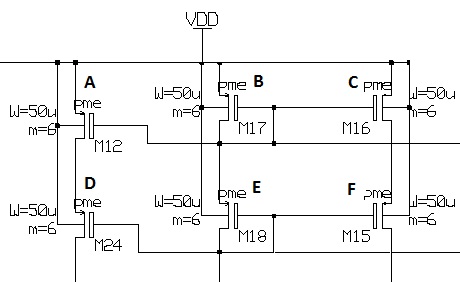
please keep in your mind that I can go more for higher transistors ratios but never less for the consideration of my main circuit. and also the length is fixed by the technology and I cannot alter it, so the only thing you can change is the width and the number of fingers

thank you very much and I will appreciate any participation of you
 

If you really want cross-coupling (requires extensive and expensive connectivity), here's my suggestion:

A B C C B A
D E F F E D

A B C
C A B
F D E
D E F

... depending on which aspect ratio you prefer.

All transistors with W=25 and f=6 (instead of m=6),
i.e. fingering instead of multiple transistors. This avoids too complex routing (it's still complicated enough!)

For the side dummies, use W=25 and f=1,
for the top & bottom dummies W=1 and f=6 . Just a suggestion!
 

Hello erikl

I can not use less transistor ratio for the consideration of the circuit design, so the actual ratio is ( (W/L)*m) and I need to keep the actual ratio as it or more, for example increase W and decrease m as L is fixed . you are free to suggest but with this condition.

in your last suggestion
A B C
C A B
F D E
D E F

it seem to be that you assumed m (or f) = 2 which will reduce the actual ratio, hope you got my problem
 

it seem to be that you assumed m (or f) = 2 which will reduce the actual ratio

No. Each of your transistors has W*m=50*6=300 . My suggestion is W=2*25*6=300 .
 

Thank you again
the minimum length I can use is W = 10 uA
you are using two factors (2 and 6 ) what are they ?

No. Each of your transistors has W*m=50*6=300 . My suggestion is W=2*25*6=300 .
 

the minimum length I can use is W = 10 uA
you are using two factors (2 and 6 ) what are they ?

m=2 (number of transistors: AA, BB, ...)
w=25µm (length of the transistors' fingers)
f=6 (number of fingers (gates) per transistor)
 
erikl, what about if would only use the factor m and keep f =1 as from my picture. could you then arrange it again
 

erikl, what about if would only use the factor m and keep f =1 as from my picture. could you then arrange it again

Of course one could. But not me: much too complicated, really doesn't make sense. Hell of a routing work which doesn't pay off!
 

It seems that you need to match B to A and C and D to E and F. Unless my designer specified that matching was critically important here I would be tempted to layout

*ACBBCA*
*ACBBCA*
*ACBBCA*

*DFEEFD*
*DFEEFD*
*DFEEFD*

* is dummy device

What geometry are you working on (0.35um, 0.13, 65nm) as issues like STI / LOD mismatch will probably have a larger effect on your mirror than your interleaving.
 
Thank you Pat for your reply,

yes I want to match A with B and C and D and E and F as all representing the same current mirror


It seems that you need to match B to A and C and D to E and F. Unless my designer specified that matching was critically important here I would be tempted to layout

*ACBBCA*
*ACBBCA*
*ACBBCA*

*DFEEFD*
*DFEEFD*
*DFEEFD*

* is dummy device

What geometry are you working on (0.35um, 0.13, 65nm) as issues like STI / LOD mismatch will probably have a larger effect on your mirror than your interleaving.
 

From the schematic posted it looks like A, B and C is a current mirror where B is the diode connected device, place this in the centre of the array. Likewise D, E and F look like the cascodes to the ABC mirror, E seems to be the diode connected device here so it should go in the mirror. Generally cascode matching is less important than the devices in the mirror.
 

Hello pat
Actually I have mentioned that this circuit is cascode current mirrror wit hsix transistors not only three. what about your first suggestion? if you have a better suggestion please put it like an array as you did before

Thank you again

From the schematic posted it looks like A, B and C is a current mirror where B is the diode connected device, place this in the centre of the array. Likewise D, E and F look like the cascodes to the ABC mirror, E seems to be the diode connected device here so it should go in the mirror. Generally cascode matching is less important than the devices in the mirror.

- - - Updated - - -

is it possible to match three transistors separately fro the other ??
 

Status
Not open for further replies.

Part and Inventory Search

Welcome to EDABoard.com

Sponsor

Back
Top