Continue to Site

Welcome to EDAboard.com

Welcome to our site! EDAboard.com is an international Electronics Discussion Forum focused on EDA software, circuits, schematics, books, theory, papers, asic, pld, 8051, DSP, Network, RF, Analog Design, PCB, Service Manuals... and a whole lot more! To participate you need to register. Registration is free. Click here to register now.

Transient logic of zener level shifter

yefj

Advanced Member level 5
Joined
Sep 12, 2019
Messages
1,505
Helped
1
Reputation
2
Reaction score
5
Trophy points
38
Activity points
9,114
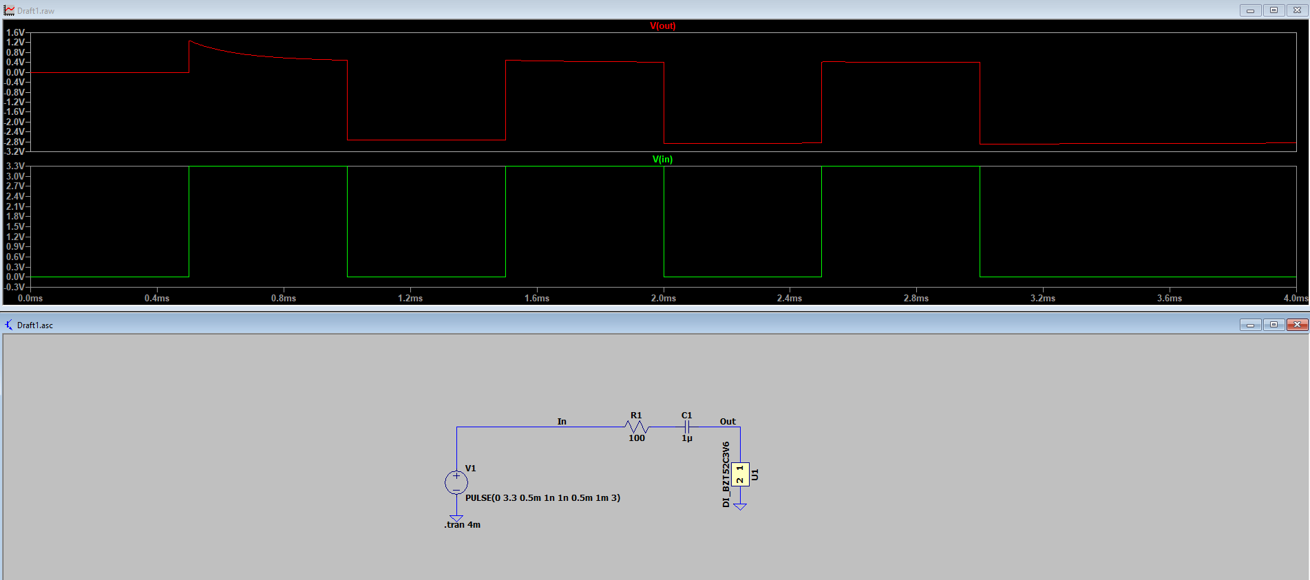
Hello, In the circuit bellow a Level shifter was made using Zenner diode.
However as you can see it drops only at the second pulse to the desired value.
Is there a way to make it do the level shifting from the first pulse?
Thanks.
1713256172793.png
 
Hi,

.. you call it Zener shifter...

but indeed the "shifting" is done by the capacitor. The Zener is just the "voltage limiter".
The capacitor needs to be charged to the desired level.

It is not perfect, because it is not useful for higher current and not useful for very low frequencies.
And as you already know it needs to be "initialized". This initialization is only possible for known input state and needs extra circuit.

Extra parts ... while not perfect.
So why not use a dedicated level shifter, an optocoupler, a digital isolator, an analog switch, or similar?

****
Especially when you want to (worldwide) share a schematic I vote for using standard symbols. A box with numbers "1" and "2" could be anything.
And if you do a simulation, then try to do it realistically .. with a load.

Klaus
 
Is you zener in backwards polarity, so its just clamping at .7V ?

1713268033512.png


The design is seeing the differentiator action of a RC to a square wave. The
peak generated by the C + R (100 ohm) + R (dynamic R Zener).

As Klaus points out you really have a clamp circuit, not a shifter.

Why do yiou have the Capacitor ? Describe goal of circuit, Vin range, frequency,
Vclamp and its needed accuracy.....load on circuit output.....


Regards, Dana.
 
Last edited:
Hello, In the circuit bellow a Level shifter was made using Zenner diode.
However as you can see it drops only at the second pulse to the desired value.
Is there a way to make it do the level shifting from the first pulse?
Thanks.
View attachment 190114
Holy cow. This is a question techs. might ask in 101 electronics.
The diode never reaches reverse breakdown voltage and acts a simple passive +ve clamp circuit.
In the diode clamp driven by a series RC + signal 0 to 3.3V you expect the diode to have two states, ON & OFF with a series resistance you can estimate for each using the datasheet. The resistance can be estimated by V/I for forward and reverse biased from the datasheet, which I expect you can read and interpolate for 3.3V.

1713273856634.png


What do you estimate for the diode Rs with a fixed voltage drop of (3.3-0.8)/ 100 ohms= I being the diode current?

All TV's take the AC coupled video signal and then clamp the "back porch" after negative sync tip using an active pulse to short circuit the load for 100 ns when the output is expected to be 0V. This serves as the video 0% IRE or "black" level reference. This is an active clamp as opposed to the passive diode clamp using a low C[pF] FET with say <1 Ohm.

Since video signals use 75 Ohm impedance and using 5 T decay times for a low steady-state (SS) error ...
Can you estimate the resistance of the switch in the ON state? R=T/C and choose C such that the output does not decay more than 1% during the Hsync period of video of 15 ms with an estimate leakage current in the OFF state of say 1uA?

Can you think of a DC coupled circuit that has a negative non-inverting level shifter function? (using a transistor with a negative Vss load)
Can you think of a way to shift the load so the negative output is no 0V and the load is now +ve so your circuit runs off a single +ve supply? is it floating?
 
Last edited:
s there a way to make it do the level shifting from the first pulse?
You can use a resistive divider at the output of the capacitor from a V- supply to ground to set the DC average level at the value that occurs when the circuit is operating.
 
You can use a resistive divider at the output of the capacitor from a V- supply to ground to set the DC average level at the value that occurs when the circuit is operating.
He is obviously resisting to use a negative supply and also if he wants to drive FET gate (this is getting old) he needs at least a 2.5x Vgs(th) =Vgs swing. Thus attenuation is not a good side effect.
--- Updated ---

Holy cow. This is a question techs. might ask in 101 electronics.
The diode never reaches reverse breakdown voltage and acts a simple passive +ve clamp circuit.
In the diode clamp driven by a series RC + signal 0 to 3.3V you expect the diode to have two states, ON & OFF with a series resistance you can estimate for each using the datasheet. The resistance can be estimated by V/I for forward and reverse biased from the datasheet, which I expect you can read and interpolate for 3.3V.

View attachment 190137


What do you estimate for the diode Rs with a fixed voltage drop of (3.3-0.8)/ 100 ohms= I being the diode current?

All TV's take the AC coupled video signal and then clamp the "back porch" after negative sync tip using an active pulse to short circuit the load for 100 ns when the output is expected to be 0V. This serves as the video 0% IRE or "black" level reference. This is an active clamp as opposed to the passive diode clamp using a low C[pF] FET with say <1 Ohm.

Since video signals use 75 Ohm impedance and using 5 T decay times for a low steady-state (SS) error ...
Can you estimate the resistance of the switch in the ON state? R=T/C and choose C such that the output does not decay more than 1% during the Hsync period of video of 15 ms with an estimate leakage current in the OFF state of say 1uA?

Can you think of a DC coupled circuit that has a negative non-inverting level shifter function? (using a transistor with a negative Vss load)
Can you think of a way to shift the load so the negative output is no 0V and the load is now +ve so your circuit runs off a single +ve supply? is it floating?
Capiche? any questions?
 
His questions are more focused (myopic) and missing all the requirements.

It was hinted on March 9th with a 10 GHz Pch power FET in a 300W RF Amp that needs a negative gate voltage pulse, which must be controlled by drain current sensing.

1713290474995.png


A common base PNP can level shift a uC logic level to negative swing load resistor with a diode clamp.
 
Last edited:
Hello Tony,Could you show an example so i could simulate such diode PNP clamp?
Thanks.

"A common base PNP can level shift a uC logic level to negative swing load resistor with a diode clamp."
--- Updated ---

Hi,

.. you call it Zener shifter...

but indeed the "shifting" is done by the capacitor. The Zener is just the "voltage limiter".
The capacitor needs to be charged to the desired level.

It is not perfect, because it is not useful for higher current and not useful for very low frequencies.
And as you already know it needs to be "initialized". This initialization is only possible for known input state and needs extra circuit.

Extra parts ... while not perfect.
So why not use a dedicated level shifter, an optocoupler, a digital isolator, an analog switch, or similar?

****
Especially when you want to (worldwide) share a schematic I vote for using standard symbols. A box with numbers "1" and "2" could be anything.
And if you do a simulation, then try to do it realistically .. with a load.

Klaus
Hello Klaus, In the circuit below,I didnt have this transient phenomena.
From the first pulse output reacted exactly as the other pulses.
the box is imported spice file of zenner diode with 3.6V reverese voltage.
pin one is anode pin 2 is cathode.
Why in one configuration it takes two pulses to reach the desired result while in the clamp circuit below i get the desired result from the first pulse?
Why the capacitor is charge and functioning from the first pulse in the circuit below while on the circuit of the first post it takes two pulses to charge?

Thanks.


1713300111268.png


1713299846105.png
 
Last edited:
Hi
In the circuit below,I didnt have this transient phenomena.
From the first pulse output reacted exactly as the other pulses.
Your statement is absolutely wrong.

While the circuit of post#1 shows to be "adjusted" within one clcock cycle ... your new circuit never gets to the same performance.

When you see the input it is peak-to-peak of 3.3V in post#1 ... and the output also gets almost 3.3V pp.

Now to you your circuit of post#9:
You also have a 3.3V pp input voltage (why these unrealistic 0.7V / 4.0V levels??) .. now look at te output: it is nowhere near 3.3V pp!!
It´s rather 1.4Vpp (Flat part to flat part).

It´s a complete differetn circuit with complete different function and levels. It´s a riddle why you modified it this way.

***

You did not state how you expect the circuit to work.
I don´t like guessing when doing electronic designs.

Klaus
 
Hello Klaus,Can i have some mathematical manual reagrding these examples so i would understand how they work exactly?
 
Hello, In the circuit bellow a Level shifter was made using Zenner diode.
However as you can see it drops only at the second pulse to the desired value.
Is there a way to make it do the level shifting from the first pulse?
Thanks.
View attachment 190114
The reason for the +1.2V leading edge pulse is that the BZT52C3V6 is conducting only as a fwd. diode with a conduction knee resistance of almost 100 Ohms. The Thevenin divider from the 3.3V voltage source of the voltage ratio matches the resistance ratio for 3.3V/100 = 33 mA. The decay to about 0.2V is because the voltage drop Vf is equal to this value at the low current after 0.5 ms. This second parameter determines the 1st negative pulse height which depends on the decayed current at time t after RC with the diode Vf.

The Zener is a poor choice compared to a power Schottky diode shown below.

The response will have 2nd order effects if the Zin of a very large FET gate are added. https://tinyurl.com/254t3hvv
https://tinyurl.com/2b7r9zyf
1717882896419.png
 
The Zener effect was named after Physicist Dr. Clarence Zener, not zenner.

Do you understand Zzt and Zzk how are measured?
What is the formula? Z = ΔV/ΔI

for I = Izt test voltage at 5 mA and I = Izk at 1 mA (start of the knee shape)

(Ohms Law for AC incremental resistance (small AC signal over DC.)

"Is there a way I could see the opening of the zenner diode in the plots below?"


In other words,
How does a conducting Zener impedance affect the pulse shape into a resistive load but with a small speed-up cap across Zener?

Use 1st principles of linear superposition.
You analyze the circuit with Zener and C1 separately then add the transfer function of each.
Use LTspice for this to understand. Then add your FET gate charge load (which will massively affect the response.

Use the mouse in LTspice to click and drag from V(before) to V(after) to add the Zener differential voltage plot. Then define another plot of the Zener effective resistance in a new plot with its voltage on the other Y axis.

The 3.3V CMOS logic of <25 Ohms sees a partially capacitive load across what appears to be a 3.6V Zener to a -2.5V biased 400 Ohm load. The datasheet specifies the Zener (AC) impedance goes from 90 to 900 ohms when bias changes from 5 to 1 mA.


This certainly looks like your pet topic. (?) Will this drive a very large PFET gate with a negative pulse, take 101...) and our challenge to guess what you are not saying.

 
Reducing current (so Zout not very good), running the Vcc closer
to max, we get :

1722799204082.png


Maybe something better than a 3906.....is OP constrained to ABT04....what is load
on output side.....better spice model for ABT....tune R1 R2 to move waveform offsets
to get higher Vohout/lesser -Volout

None of these options as good as a design specific integrated translator....
 
Last edited:

LaTeX Commands Quick-Menu:

Similar threads

Part and Inventory Search

Welcome to EDABoard.com

Sponsor

Back
Top