Continue to Site

Welcome to EDAboard.com

Welcome to our site! EDAboard.com is an international Electronics Discussion Forum focused on EDA software, circuits, schematics, books, theory, papers, asic, pld, 8051, DSP, Network, RF, Analog Design, PCB, Service Manuals... and a whole lot more! To participate you need to register. Registration is free. Click here to register now.

[SOLVED] Transformers on a PCB

Status
Not open for further replies.

inklen

Full Member level 1
Full Member level 1
Joined
Oct 18, 2019
Messages
98
Helped
0
Reputation
0
Reaction score
0
Trophy points
6
Activity points
768
Hey guys!

I've just started with electronics and I made this PCB for an amplifier which contains 2 transformers. Here's the layout (with some SMD components):
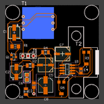
pcb.png

The transformers are on the opposite side.
This is my 2nd PCB and since this is an amplifier I wonder how the transformers affect the circuit (if it does at all). For example, look at the U1 IC which resides exactly under the transformer. Can this cause any problems? Reading the books, I think it's not going to affect anything as this is not an RF or UHF circuit. What do you think?

(the size of the PCB is 45x45 mm).

Thank you.
 
Last edited by a moderator:

Hi,

It does not depend on whether your circuit produces HF or not, it depends whether your circuit reacts on HF. And this depends on what exactly U1 is.

In either case: In times of many HF sources around (cellular phone, WiFi, bluetooth ...) I´m more concerned that you don't use a solid GND plane.
I expect EMC problems - independent of transformers.

Read the U1 datasheet and look for design notes and application notes at the manufactrer´s internat pages.

Klaus
 

Thank you. I read couple of articles about this. So, here it is with the ground plane:

pcb-ground-plane.png

Since I have a single layer board, can I make it better?
 
Last edited by a moderator:

Hi,

We are talking about HF. Thus this still is far away from being a GND plane.
All the traces have the same length as before ... and for HF the width doesn´t play much a role.

Simple method: Use double layer. Make the whole layer GND without any other traces/signals.
Use short traces to connect each single GND line with a via to GND plane.

****

Are you sure your "secret U1" has no GND connection?
I assume the U1 connection is wrong/inclomplete. I see only one resistive connection to the other circuit, any other signals are either floating or have a capacitor in series.

****

But as long as you hide most informations like part names, values, schematic, description ... it´s useless to go on guessing.

Klaus
 

Thanks for the advice!

Well, I've never done double layer yet... I thought I'd go with the single. I have to read something about via's, maybe I'd go that route.

U1 is just LM386. It's connected to ground via R6 and bypassing C6 (100n). Not sure why R6 is here which is just 10R.

But I created a prototype on a prototype board and it works. But yes, it's noisy. Hopefully, because of a long long wires and ... well, prototype board.
 

Hi,

U1 is just LM386. It's connected to ground via R6 and bypassing C6 (100n).
No!

Repeated:
But as long as you hide most informations like part names, values, schematic, description ... it´s useless to go on guessing.

Klaus
 

Yikes!!! You're right!!! Grrr... I have to change everything!

Damn, I had everything correct on the prototype... and then screwed up the circuit in the software :/

- - - Updated - - -

Fixed. That's the best I can do for now:

pcb-fixed.png
 

An LM386 is an audio amplifier, with significant gain.

Your transformer appears to be a powerline 50/60 Hz device with an EI core. Such transformers are notorious to produce significant stray fields.

Your audio amplifier will very likely suffer from lots of hum.
 

No, both transformers are audio and they're for impedance matching.

But I was thinking to isolate them as they're on the other side of the board. I hope this will remove the hum.
 

The magnetic stray field of audio transformers isn't expected to cause problems in your circuit, unless it involves very high gain (e.g. G>100). If magnetic coupling occurs, it will be to trace loops, not ICs or other lumped components.

A ground plane may be suggested or even necessary for your circuit, but the problem isn't particularly related to using transformers.
 

Thank you guys for your valuable info! I had to go and read about ground plane and PCB design overall. It's not that I understand everything now but it's a good start.

Since I can't make a double sided PCB for now, I'll go with the single side and see what I get in reality. So, this is going to be the first prototype!
 

Status
Not open for further replies.

Similar threads

Part and Inventory Search

Welcome to EDABoard.com

Sponsor

Back
Top