Continue to Site

Welcome to EDAboard.com

Welcome to our site! EDAboard.com is an international Electronics Discussion Forum focused on EDA software, circuits, schematics, books, theory, papers, asic, pld, 8051, DSP, Network, RF, Analog Design, PCB, Service Manuals... and a whole lot more! To participate you need to register. Registration is free. Click here to register now.

Transformerless Grid connected Inverter ZCT technique

Status
Not open for further replies.

faiz khan

Member level 1
Member level 1
Joined
Apr 30, 2015
Messages
35
Helped
0
Reputation
0
Reaction score
0
Trophy points
6
Activity points
263
I am doing project on Transformerless grid connected inverter based on zero current transition technique.this topology is similar to H6 inverter ,the main difference is we have to use to use two resonant circuit with auxilary switches in order to achieve Zero current switching of the main high frequency switches S5 and S6...
The problem is am unable to get the exact modulating signals to the high frequency and auxilary switches which i required.
can anybody help me in providing the simulink model to obtain required pattern.am attaching the required modulating waveforms .

thanking you

- - - Updated - - -

frequency of the carrier signal is 50khz. The circuit diagram for my project is also attached...please help me friends with simulink model for the control circuit for this circuit whose modulation pattern is attached above..

thank you
 

Attachments

  • modulating.JPG
    modulating.JPG
    50.5 KB · Views: 131
  • ckt.JPG
    ckt.JPG
    28.3 KB · Views: 135

Your diagram of waveforms is typical for the H-bridge arrangement at the output section of your schematic. However a different operation appears to happen in the left half of your schematic. Is this the section which you are asking about?

What methods have you tried so far?
 

PWM generation by comparing the waveforms same as in the figure....i tried it in MATLAB.
i used simple sine wave and by using switch i got the positive sine pulses and compared with the reference waveform...but i am not getting the exact pulse pattern what i required..
As it is a zct technique employed inverter , here the above waveform is for generation of pulses for high frequency main switches and below waveform is to provide pwm pulses for auxilary switches which are responsible for turning off of the high frequency main switches .there will be some overlap between the pulses of main and auxilary switches because it will take some fraction of time to become current through main switch to be zero at that moment only main switches will be turned off....
 

grid connected inverter

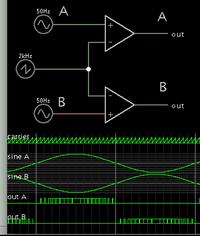
Your switching signals must always obey the grid waveform. By modulating it with your sawtooth waveform, this generates the control signals you need for mosfets S1-2-3-4.

This diagram shows how the waveforms interact.


The op amps must have a bipolar supply, but their output must be rectified so the polarity is correct for driving the mosfets.

Whenever you put N-devices on the upper side of the H-bridge, you must drive them with a bias voltage which is high enough to turn the N-device on. For this reason you may want to consider putting P-devices at the high side.
 

Status
Not open for further replies.

Part and Inventory Search

Welcome to EDABoard.com

Sponsor

Back
Top