d123
Advanced Member level 5

Hi,
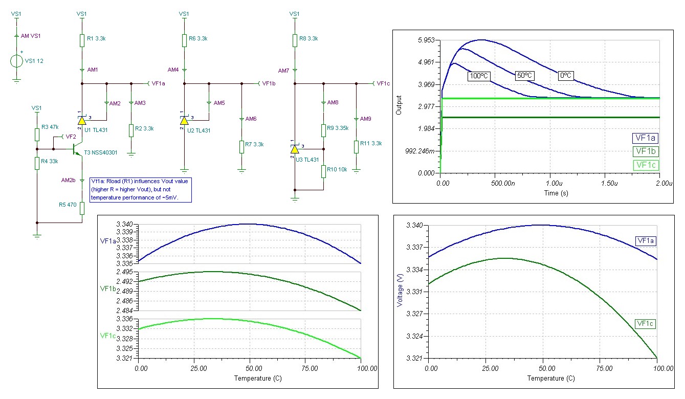
Does anyone with deep enough knowledge of, and long-running experience of using, the TL431A or even TL431C versions (TO-92) consider that this circuit adaptation idea to reduce dVref/dT across a wider temperature range than 0ºC to 60ºC (here 100ºC was chosen) is plausible and potentially effective as a temperature-compensation method?
And, therefore, credible and feasible in the real world on a PCB that is conscientiously laid out? I'm talking of a single board and selecting components (and with post-soldering trimming of R1, R3, R4, R5, as needed) not mass production. Bonding TL431 T0-92 case (bent leads) to NSS40300 SOIC case with that grey gunk seems very feasible in order to more or less match Tamb experience of both parts.
Do the simulation results seem sufficiently realistic or are they overly-idealistic?
I know TL431 drifts some 40mV to 60mV across its temperature range of use with a stable supply. Iref goes from 2uA to 4uA.
Resistors are 100ppm and making them 10ppm didn't alter the results at all. VF1a has somewhat nasty and 'slow' start-up behaviour... Also, the rise in Vref to ~3.3V seems irrelevant if 2.5Vref is not a vital 'must have'. I also see that from 0ºC to 60ºC such an addition would be completely unnecessary as the TL431 only theoretically changes by some 3mV across that range.
Previous attempts included e.g. subtracting or adding a temperature-dependent current to pin 3 (adjust) and that made no improvement at all. This version alleges it could.
Thank you.
