alexxx
Advanced Member level 4

Hello.
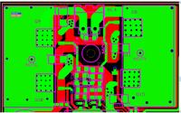
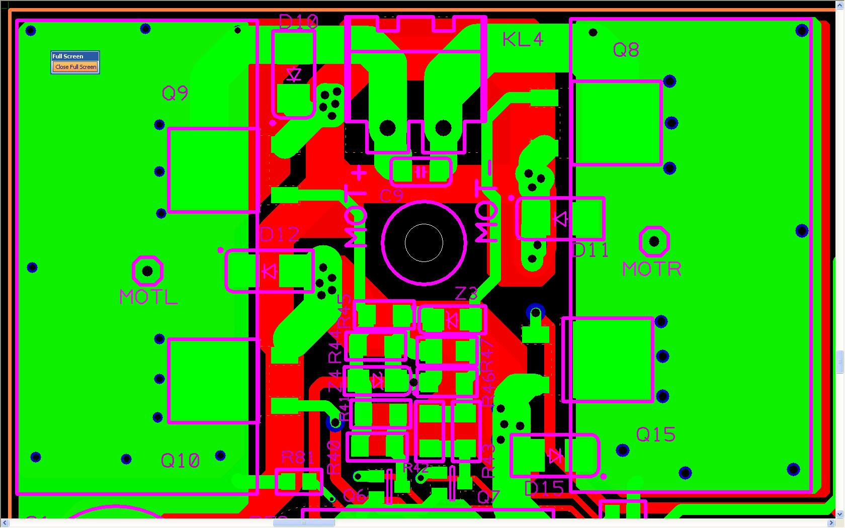
The below part is an H-bridge layout, 2 layers. FETs are SMD and use the printed board as cooler.
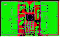
Now after some searching I thought that maybe there is a better way from thermal point of view, having less vias.
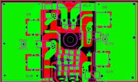
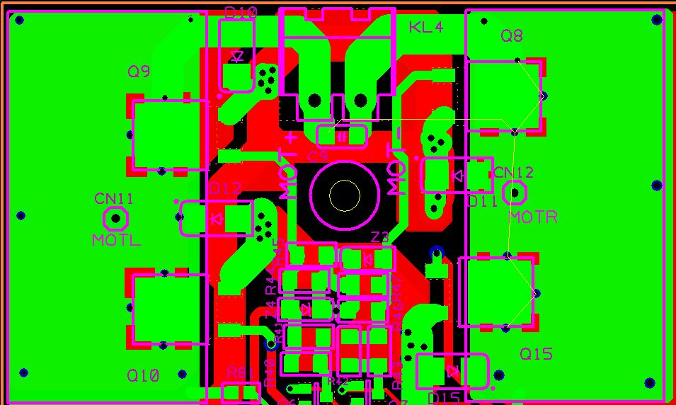
Adding thermal relief, it should look like that:
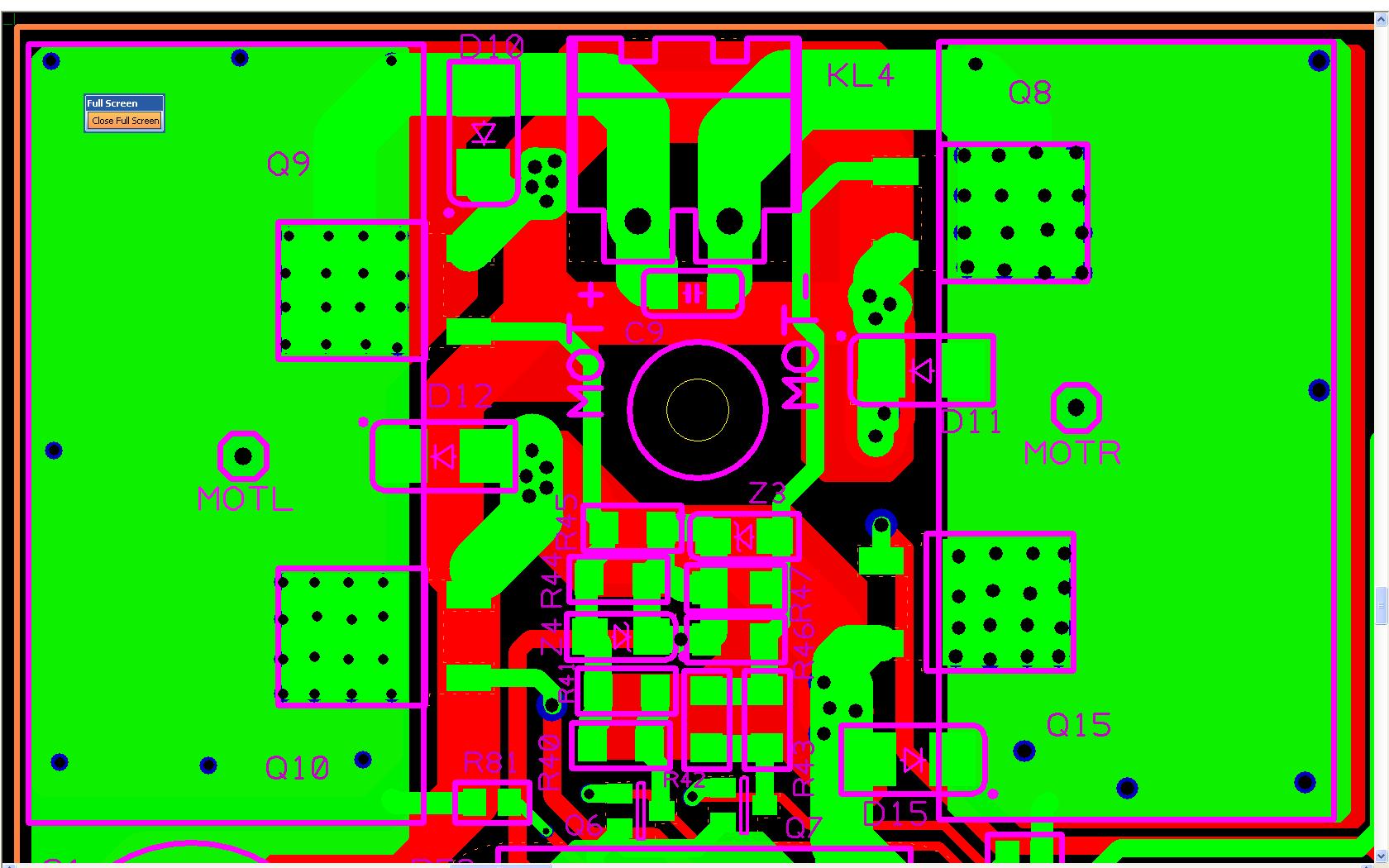
What do you think? Will thermal behaviour be improved?
Thanks,
Alexandros
The below part is an H-bridge layout, 2 layers. FETs are SMD and use the printed board as cooler.
Now after some searching I thought that maybe there is a better way from thermal point of view, having less vias.
Adding thermal relief, it should look like that:
What do you think? Will thermal behaviour be improved?
Thanks,
Alexandros

")

