Continue to Site

Welcome to EDAboard.com

Welcome to our site! EDAboard.com is an international Electronics Discussion Forum focused on EDA software, circuits, schematics, books, theory, papers, asic, pld, 8051, DSP, Network, RF, Analog Design, PCB, Service Manuals... and a whole lot more! To participate you need to register. Registration is free. Click here to register now.

Thermal pad construction on pcb

Status
Not open for further replies.

Rajinder1268

Full Member level 3
Full Member level 3
Joined
Mar 20, 2021
Messages
162
Helped
1
Reputation
2
Reaction score
4
Trophy points
18
Activity points
1,228
Hi all,
I am doing my first layout using the ESP32 and was looking for some advice.

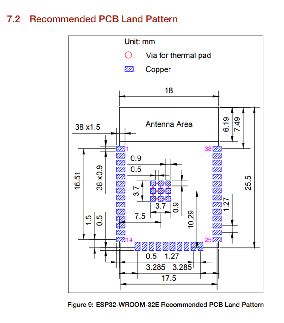
I have created a footprint based on the land pattern below:
1656254125002.png


My question is how do I connect the Vias that are placed in between the 9 pads? Do I connect them all straight to GND? Do I really need the vias, Or can I simply delete them and make one copper pad (instead of 9 smaller pads), then run a small track from this pad and track to a via to GND?

It gets a bit confusing as the datasheet mentions:

1656254271391.png


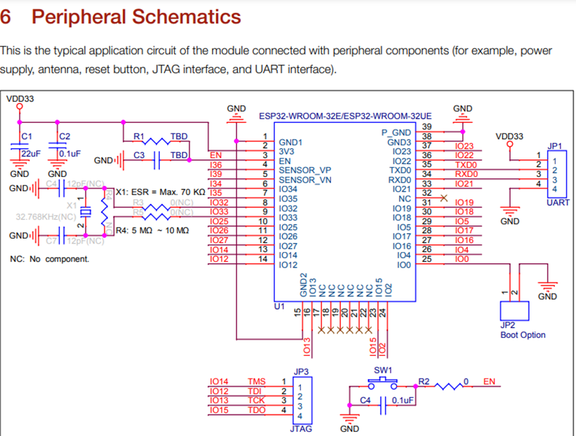
On the schematic diagram for the ESP32 devkit pad 39 (thermal pad) is connected to GND (see below). Has anyone used this device and done a layout?
1656254517179.png


Can anyone assist?
Thanks
 

If you don’t have the vias, how will the pad connect to ground?

You could also have a single solid pad with vias in the pad, but this is a little harder to solder.
 

If you don’t have the vias, how will the pad connect to ground?

You could also have a single solid pad with vias in the pad, but this is a little harder to solder.
Hi
Could I create a larger copper pad and then have small tracks with vias on the periphery connected to GND.
In the data sheet it mentions the copper pad does not need to be soldered.
Do I need to connect each via to one of the 9 pads using a small track?
--- Updated ---

Surround the square pads with 12 small vias and pour them with a copper.
Sounds good ?
Not sure what you mean.
Do I connect the vias with small tracks to the 9 pads, the vias making the connection to GND?
 

Hi
Could I create a larger copper pad and then have small tracks with vias on the periphery connected to GND.
In the data sheet it mentions the copper pad does not need to be soldered.
Do I need to connect each via to one of the 9 pads using a small track?
--- Updated ---


If the Copper Pad does not need to be soldered, simply place a copper pour with many thru vias. Of course you should open solder resist mask to make IC less warm.
 

Hi
Could I create a larger copper pad and then have small tracks with vias on the periphery connected to GND.
In the data sheet it mentions the copper pad does not need to be soldered.
Do I need to connect each via to one of the 9 pads using a small track?
--- Updated ---


Not sure what you mean.
Do I connect the vias with small tracks to the 9 pads, the vias making the connection to GND?
the data sheet says the pad doesn’t HAVE to be connected, but you’ll get better performance if it is. If you’re going for better performance, then solder the pad. Going to the trouble of creating a land pattern with a bunch of copper and vias, and then not soldering it is a waste of time.
 

the data sheet says the pad doesn’t HAVE to be connected, but you’ll get better performance if it is. If you’re going for better performance, then solder the pad. Going to the trouble of creating a land pattern with a bunch of copper and vias, and then not soldering it is a waste of time.
Hi,
I intend to connect to GND. I am not entirely sure what the best method would be. Do I connect the via to GND then run a small track to one of the 9 small pads? I am not sure. Can you assist?
 

unless you've got the world's worst PCB house, there should be no problem putting the vias right in the pad. Check with your vendor.
 

unless you've got the world's worst PCB house, there should be no problem putting the vias right in the pad. Check with your vendor.
I will but from past experience they do not have the knowledge on how to do this. Hence my recommendation for the vias to GND and then run short tracks to the 9 pads, that should work I think.
 

I will but from past experience they do not have the knowledge on how to do this. Hence my recommendation for the vias to GND and then run short tracks to the 9 pads, that should work I think.
I think the point of the ground pad in this case is for thermal, not electrical, purposes. So, a thin trace to a via is not going to work well.
 

I think the point of the ground pad in this case is for thermal, not electrical, purposes. So, a thin trace to a via is not going to work well.
If that is the case then do I just connect the vias to the GND plane?
 

Hi,

You don't need a "GND" plane, you just need copper to spread the heat.
The electrical connection is not important for this.

While you don't need a GND plane, you still can use it, if you have.
A xxx-plane is copper ... and copper spreads the heat.
The vias (copper) are used to spread the heat from one copper layer to the other. So if you want the heat to go from TOP layer to BOTTOM layer you need copper. The more coper the better the thermal conductivity. Use multiple vias, use big vias (as long as it does not create other problems)
But if the heat now is at the bottom side ... you still ned a big copper area there to spread this heat.

Klaus
Hi
my confusion is in the understanding. I have 9 small copper pads and in between them vias. How do I connect/track this up? My second layer is GND on a 4 layer PCB. Do I need to connect only the vias to the GND plane? What about the 9 pads of copper that I have?
 

Hi
my confusion is in the understanding. I have 9 small copper pads and in between them vias. How do I connect/track this up? My second layer is GND on a 4 layer PCB. Do I need to connect only the vias to the GND plane? What about the 9 pads of copper that I have?
Posts 12, 10, 8, etc. keep telling you what to do. You keep ignoring the advice.

1) you need copper to dissipate the heat.
2) it doesn’t HAVE to be connected to ground plane
3) the vias don’t dissipate heat. they need to be, somehow, connected to the pad of the device. that‘s what the copper pads are for.
Hi,
Sorry for my lack of knowledge in this area.
So the pads can remain as they are just copper. Is there any special requirements for the thermal via? Tented? Where do the vias need connecting too?
 

Status
Not open for further replies.

Similar threads

Part and Inventory Search

Welcome to EDABoard.com

Sponsor

Back
Top