Continue to Site

Welcome to EDAboard.com

Welcome to our site! EDAboard.com is an international Electronics Discussion Forum focused on EDA software, circuits, schematics, books, theory, papers, asic, pld, 8051, DSP, Network, RF, Analog Design, PCB, Service Manuals... and a whole lot more! To participate you need to register. Registration is free. Click here to register now.

the npn with two emitters

Status
Not open for further replies.

poweric

Member level 5
Member level 5
Joined
Oct 29, 2006
Messages
80
Helped
3
Reputation
6
Reaction score
0
Trophy points
1,286
Visit site
Activity points
1,733
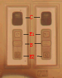
t he NPN has two emitters one baser one collector .

one of the emitters connect the baser,
the logic signal (7v) input the baser and the other emitter as the output signal whats the function of it
i dout know


so can you help me
 

havent heard of this type of connection before but i think it is used to increase the output current capability using that kind of positive feedback... if you post the circuit it would be helpful to understand...
 

96_1193975501.gif


19_1193975799.gif


the photo as above
the E1 have connected the B

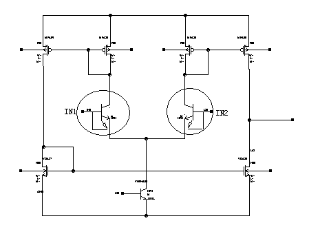
you can see the schemtic in the 2nd photo

the IN1 and IN2 are the logic signal (max=7v) the power supply is about the 10V

what is the function of it
 

as far as i know since the other emitter is connected like that it would be acting like a capacitor and it would reduce the glitching of that transistor output....
 

Hello Poweric,
1 reason could be that the 2x emitter NPNs may be having a better matching in the process also do you know are these vertical bipolars or lateral?
 

I think it was used to amplify the current.


Regards,

Necolei
 

to aryajur
the NPN is the vertical device. the macth is the function of the layout but do the method have the electricl function in the circuit

Added after 26 seconds:

to aryajur
the NPN is the vertical device. the macth is the function of the layout but do the method have the electricl function in the circuit

Added after 3 minutes:

to A.Anand Srinivasan
thanks for your help one member of our team have also think it as the capacity ,but we dout know why?
can you give me some paper about this thesis i have found nothing
 

i just tried analysing the circuit you have posted that is all... the other emitter is reverse biased so it is obvious that it is supposed to be a capacitor,,,, there must be more than one reason for this... can u post the whole document that you got this circuit from....
 

i am sorry for leaving a long time the circuit is come from the motor driver the power suppy is the 38V
 

do you mean that the input signal IN1 and IN2 come from motor drive??? if so can u please the motor drive circuit or the part of the motor drive connected...
 

Do the process have a single emitters npn?

Is it to increase the gain of the npn differential stage?
 

the IN1 is the output PIN of the circuit it is come from the ST l6506 output the IN2 is the reference Voltage of the this circuit
 

the ST16506 part isnt helping me... i wasnt able to find anything about it... can u post the circuit or its datasheet....
 

Status
Not open for further replies.

Part and Inventory Search

Welcome to EDABoard.com

Sponsor

Back
Top