jokincifu
Newbie

Hello everyone,
To give you a context of what I am simulating and why, the ultimate goal is to build a Reconfigurable Intelligent Surface with multiple unit cells to reflect the signal in different directions. I am using the CST Studio 2019 tool for the simulations, using Frequency Domain Solver simulations with Floquet ports.
I am simulating a rectangular unit cell at the frequency of 9.6 GHz where the reactance value can be changed to modify the phase of the reflection coefficient.
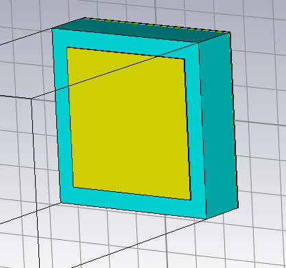
For this, I have designed a unit cell of 5x5mm, with a substrate (MT-40) height of h=1.5mm, and a top metal (Annealed Copper) reflector of 4x4mm, as shown in the following image:

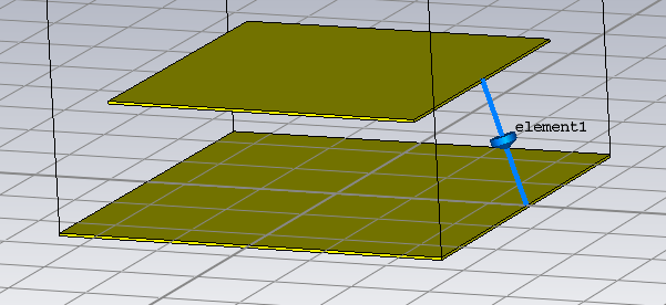
To modify the reactance of the unit cell, I inserted a finite element (RLC serial type element, but only giving value to the C parameter, in order to have a capacity) into the cell. As an ideal first step (to see if the element has effect on the response), I placed the element between the upper and lower metals (Ground), as shown below:


In the image above it can be seen the values of the phase of the S11 (refering to reflection from the cells) by modifying the value of the capacitor, proving that the capacitance has an influence on the reactance of the unit cell.
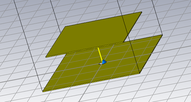
In order to design a more realistic unit cell (for future implementation of the cells), I inserted a metallic via from the metal top patch to the bottom patch, in which I drilled a hole (0.2mm radius) so that the via goes through both the substrate and the bottom patch, thus connecting the capacitor between the via and the bottom patch, as shown in the following image:

To give more information:
-The via and the top patch are a complete component (created with the Boolean>Add tool).
- The hole in the bottom patch was created by using a cylinder of vacuum material and subtracting it (Boolean>Substract) from the bottom metal.
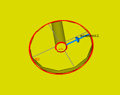
- The capacitor has been placed by selecting the circular edges of the via and the hole:

The following figure shows how the value of S11 changes with the capacitor values. It can be seen that the capacitor has no effect on the response of S11, as if it does not generate any capacitance in the unit cell.

The S11 response that should be achieved with the via should be very similar to the previous case, it should vary a little (due to the inductance introduced by the via in the cell), but for practical purposes it should be similar. However, it is observed in the image that the results are not similar, and that no matter the value introduced in the capacitance, this has no effect on the response of the cell.
I have been thinking a lot about the problem, I deduce that it may be related to the way of simulating, but I don't know where exactly the failure may be. Thank you in advance.
P.D. I attach also the .cst files (the capacitance connected in an ideal way (_Varicap) and using the via (_Via)), in case someone wants to simulate it/change some things.
To give you a context of what I am simulating and why, the ultimate goal is to build a Reconfigurable Intelligent Surface with multiple unit cells to reflect the signal in different directions. I am using the CST Studio 2019 tool for the simulations, using Frequency Domain Solver simulations with Floquet ports.
I am simulating a rectangular unit cell at the frequency of 9.6 GHz where the reactance value can be changed to modify the phase of the reflection coefficient.
For this, I have designed a unit cell of 5x5mm, with a substrate (MT-40) height of h=1.5mm, and a top metal (Annealed Copper) reflector of 4x4mm, as shown in the following image:
To modify the reactance of the unit cell, I inserted a finite element (RLC serial type element, but only giving value to the C parameter, in order to have a capacity) into the cell. As an ideal first step (to see if the element has effect on the response), I placed the element between the upper and lower metals (Ground), as shown below:
In the image above it can be seen the values of the phase of the S11 (refering to reflection from the cells) by modifying the value of the capacitor, proving that the capacitance has an influence on the reactance of the unit cell.
In order to design a more realistic unit cell (for future implementation of the cells), I inserted a metallic via from the metal top patch to the bottom patch, in which I drilled a hole (0.2mm radius) so that the via goes through both the substrate and the bottom patch, thus connecting the capacitor between the via and the bottom patch, as shown in the following image:
To give more information:
-The via and the top patch are a complete component (created with the Boolean>Add tool).
- The hole in the bottom patch was created by using a cylinder of vacuum material and subtracting it (Boolean>Substract) from the bottom metal.
- The capacitor has been placed by selecting the circular edges of the via and the hole:
The following figure shows how the value of S11 changes with the capacitor values. It can be seen that the capacitor has no effect on the response of S11, as if it does not generate any capacitance in the unit cell.
The S11 response that should be achieved with the via should be very similar to the previous case, it should vary a little (due to the inductance introduced by the via in the cell), but for practical purposes it should be similar. However, it is observed in the image that the results are not similar, and that no matter the value introduced in the capacitance, this has no effect on the response of the cell.
I have been thinking a lot about the problem, I deduce that it may be related to the way of simulating, but I don't know where exactly the failure may be. Thank you in advance.
P.D. I attach also the .cst files (the capacitance connected in an ideal way (_Varicap) and using the via (_Via)), in case someone wants to simulate it/change some things.

