Continue to Site

Welcome to EDAboard.com

Welcome to our site! EDAboard.com is an international Electronics Discussion Forum focused on EDA software, circuits, schematics, books, theory, papers, asic, pld, 8051, DSP, Network, RF, Analog Design, PCB, Service Manuals... and a whole lot more! To participate you need to register. Registration is free. Click here to register now.

[SOLVED] Telit Gsm Module Noise Problem

Status
Not open for further replies.

kcagiran

Junior Member level 1
Joined
Apr 26, 2018
Messages
16
Helped
0
Reputation
0
Reaction score
0
Trophy points
1
Activity points
145
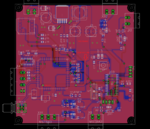
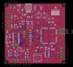
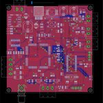
I am electronic engineer stundent and i have an iot project thesis. I designed 2 layer pcb that reads inputs and making phone call on GSM. Teorically every single things works well. But there is huge noise when make phone call. I can hear noise PCB's and phone's speaker.

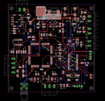
I am uploading 2 picture, 1st picture my first design and realy bad, because long and 90degree line are terrible. And my antenna line is under GSM module vcc line.

But 2nd pcb design is better, but still i have noise problem.

Please help me about solving this problem. I really need your any suggestions and any advice.

Thank you!
 

Attachments

  • 1ST PICTURE.jpg
    1ST PICTURE.jpg
    210.4 KB · Views: 278
  • 2ND PICTURE.png
    2ND PICTURE.png
    351.4 KB · Views: 308

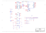
Only a snapshot of the board is not very useful to evaluate the system as a whole once we have no clue of what each component is; I presume you can share here the schematic of the board, otherwise there will have little to help you.
 
View attachment schematic.png

Thank you for your reply sir!

Here is my schematic, i prefered switch regulator and placed every components which is recommended in telit hardware user guide. In my school my teachers can not give real advice to solve noise problem. They only said to me to choice lineer regulator. But I know i can use switch regulators because telit hardware guide tells it to me.
 

Hi,

Yet another PCB layout where there is no GND plane.
A copper pour is no GND plane....


Klaus
 
I admit that I have little experience with audio applications, and I also have no clue of what IC is the one you are using (P/N is not present in schematic), but at a glance, it sounds weird to have 1M resistor at the MIC- pin. In addition, I would expect both MIC nets straight from the microphone to the IC pair pins, not grounded close to digital pins. Another thing is that you are using the same connector either to speaker and microphone, which carries power and weak signals; anyway I may be wrong in that assumptions. Can you describe what kind of noise you hear ?
 
11.png

22.png

Thank you for your reply!

these are PCB layouts without GND and VCC planes.

there are GND planes at bottom and top. Only have a VCC plane at 2nd PCB. Should the GND plane continuous, i mean without any split VCC planes?
 

The problem is coming from "the design", not PCB yet..
You connected everything to a single VCC.That's a fatal error.Because GSM module consumes huge current and it craps whole VCC line..It should be separated.GND connections are also important and ti has to be done through many nodes.
Speaker driver IC needs a clean VCC and GND.
In additional to, there is uC that craps also VCC line ..
There isn't decoupling capacitors for HF components ( nF and pF range )
so on..
Pay attention to decoupling capacitors,GND connections.And separate VCC lines-if applicable- and use private regulator circuits for each sensitive block.

Look at that schematic that is similar to your project.Even-though the schematic is not complete but it will give you an insight.
minerva_01-1.png
 
Last edited:

Thank you for your answer BigBoss!

These tricks will make me better no doubt! Huge thanks again!

Yes i have think using private regulators before, but this time i need to design with these components.
But i used 100nF decoupling capacitor at regulator output. I thought it ll a solution for me. But as you told i have fatal error like using 1 VCC line for each IC. Thank you! I ll design it again as soon as possible and i believe the problem will be solved. After i ll use private regulators for each IC, so i need to upgrade my schematic for the reason that it ll happen after new design.

Huge thanks to all of you! This is my first experience in here and you are amazing!
 

Hi,

Designing a PCB layout for sensitive audio signal and the same time a switching power supply (which generates noise) and a GSM modem (which also generates noise) surely is a hard job.

Two important things:
* You need to "analyze" the noisy signals (in your mind) as HF AC signals, the DC resistance is of minor interest.
* and: a noisy signal doesn't stop at the capacitor. There is always a current_return_path. In my eyes it needs to be treated more sensitive than the noisy signal path. The reason is that the signal path is limited in size, in lenght and in the connectec (influenced) parts. The return path often is the GND signal. Every part that is connected near the current_noise_return_path will be influenced.
There are several ways so keep the influence low:
- keep the return path low impedance --> a rock solid GND plane. My assumption is that your copper_pour_GND may case up to 100 times higher GND_voltage_noise that a true GND plane.
- keep the enclosed area of noise signal and it's reurn path as small as possible
- for lenghty (power) signals: filter them on both sides so you can treat the trace as noisevfee DC signal
- keep noisey signals apart from sensitive signals (part placement)

You need to be aware of the noise sources and how to keep the influence to sensitive signals low.
* there are voltage noise signals with high dV/dt which means very sharp edges. Like the switching node of your SMPS. Usually one tries to filter them locally, but this is not possible with this node. To minimize the influece (mostly capacitive effects) you need to keep the node area small. A polygon is counter productive here.
Move the diode, the IC and the L in close proximity. Best singal routing order is: IC --> D --> L
* and there are current_noise sources. They cause inductive influence. To minimize the influence to other signals:
- keep the signals apart
- keep the noisy signal short
- filter the noisy signals
- route sensitive signals in 90°angle to the noisy signals
- maybe consider filters at the destination of the sensitive signals.

If you can upload your EAGLE files I can show you how to improve your PCB layout (you may choose which section: SMPS, or audio, or uC or GSM.)

Klaus

- - - Updated - - -

Added:
I don't see the need for linear regulators. For sure they will help (especially with bad PCB layouts).
I've done a lot two sided or 4 layer PCB layouts with 16bit ADC and SMPS while the ADC is noise free down to the datasheet specifications.

Klaus
 
Huge thanks for be interested sir KlausST!

I saved all these priceless notes. And I will implement to my project as soon as possible.

You know i need to much time to understand electronics, but need to start somewhere like this.

***I added my EAGLE (brd) and (sch) zip files. If possible i want to hear your PCB layout informations, thank you!
 

Attachments

  • thesis.rar
    110.6 KB · Views: 130

Taking a look at some Telit module-based cellular phone schematics, I was not able to find any that were using the previously mentioned resistor at the MIC(-) input. Obviously this does not mean that your scheme is wrong, since the inner circuitry of the peripherals of each OEM module may be different, but I'd bet that if you replace the resistor R15 (1M) with a jumper (0R0), the noise would be quite reduced.
 
Thank you for answer andre_teprom!

I am using opamp that name is TL071 for amplifie the electrec microphone. This opamp has only 1 output that name is Mic+. But my gsm module has mic+ and mic-. After my document research, find some informations about it, if you are using only 1 input (Mic+) at the GSM module, you should use 1M resistor to your Mic-. For the reason that i am using it.

But i ll do your advice and examine the noise level. 1st i ll swap 1M resistor with 0ohm, and 2nd i ll make Mic- to open circuit. I think need to examine 2 situation with your advice.

Thank you for helping..
 

I am using opamp that name is TL071 for amplifie the electrec microphone.

So things became a little bit difficult to perceive now, because we can not know whether the noise comes from the other board, the wiring between them, or due to a bad coupling. In that case, I would not recommend to make a test leaving the circuit without any resistor at the MIC(-) once the 1M is virtually an open circuit. So, between the output of the TL071 and the MIC(+), is there a DC level decoupling capacitor? Are the microphone connections made with short and twisted cabling and wrapped with a grounded mesh?
 
Thank you for answer andre_teprom!

yes there is decoupling capacitor and i use this microphone amplifier pcb with another pcb's before. It gives really clear sound.

(By the way i tested my main PCB with directly connect speaker and microphone ot many times.)

Now started to design new pcb, can you evaluate it later, if possible?
 

pcbeda.png

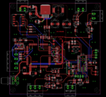
This is my last design, i add decoupling capacitors to VCC for GSM module and i placed it close to gsm as posible. I draw voice lane curved and, SPK+ and SPK- lines have same length. I have calculated the line width for GSM max 2A rule. Hope this pcb has better performance then the previous.

If it work good enough, i ll start to develop new pcb that has special regulator for each IC.
Thank you!
 

Hi,

sorry for late reply.

After reviewing the PCB layout from post#10 I saw the GND plane on the bottom side wasn´t that bad. For sure it could be improved.

But the new design is better.
Some itemes to improve:
* set your GND vias close to the GND pins (not in the center of a copper pour, this just makes the current path longer). Do it like the vias at the modem close to the antenna. Here you correctly set the via directely to the modem pad.
Especially where you expect high frequency or high current pulses. --> vias as close as possible to the pads of: C2, C3, C4, C5, C7, C8, D1, IC2, PAM2 .. and every GND pad of the modem.
Additionally move C7 closer to the modem.
Generall: move every VCC ceramics capacitor as close as possible to it´s corresponding IC VCC pin. And connect the other side of the capacitor as close as possible with a via to GND
(especially PAM and uC)

Klaus
 
Huge thanks for your good advices. The new designed PCB's are about to arrive to me, and when i try it i ll share all experience here.

***By the way, i ll start to design new ''Last design V2'' as soon as possible with your advices.

You have been very helpful..

Thank you

- - - Updated - - -

Byt the way, i can not understand one thing, you said ''And connect the other side of the capacitor as close as possible with a via to GND''
I have top and bottom GND polygon, and all capacitors have connection between top GND. You mean, connect them with via to bottom polygon to?

In the picture as you see the C3 capacitor is connected to top layer GND, do you mean add via to connect C3 to bottom GND also?capacitor.png
 

I supposed i have gnd plane at top. I defined that top copper pour as GND but now i see its actually not GND plane... You said it before but just right now understand what you mean.

the top copper pour that defined as a GND, aint it mean more GND place? If you use top Copper pour GND that will provide you more GND copper space with bottom GND plane? Is it unnecesary?
 

Hi,

Byt the way, i can not understand one thing, you said ''And connect the other side of the capacitor as close as possible with a via to GND''
I have top and bottom GND polygon, and all capacitors have connection between top GND. You mean, connect them with via to bottom polygon to?

In the picture as you see the C3 capacitor is connected to top layer GND, do you mean add via to connect C3 to bottom GND also?

as already said in post#4:
A copper pour is no GND plane....

The TOP is a copper pour - it is cut in pieces, thus see it as wires not as GND plane.
But your BOTTOM plane is a GND plane.
--> add a via as close as possible at each TOP GND to get shortest connection to BOTTOM GND plane.

******

I´m no friend of copper pour at all. (personal taste), I rather connect each TOP GND signal directely to BOTTOM GND plane.

Klaus

- - - Updated - - -

added:

Many people see a signal as if it has a beginning and an end... but every signal need a return path. (Especially HF paths, pulsed signals, EMI, EMC...)
Thus one should treat every signal as a loop. In most cases the return path is via GND.
And (one of the) the best return path follows exactly the signal path but on the opposite (next) layer. In your case the bottom layer.

TOP copper pour can not fulfill this recommendation.
But a solid GND plane can. But every cut in the BOTTOM layer (that is in the area of the TOP signal path) makes things worse. It forces the return current to leave it´s optimum path.


Klaus

- - - Updated - - -

Hi,

Is it unnecesary?

My opinion:
Nowadays with HF, SMPS and/or high dV/dt or dI/dt signals...you can´t do without a proper GND plane. The risk for EMI/EMC problems is too big. The risk for bad performance (noise) or malfunction is too big.
There is no problem if a hobbyist´s circuit will fail ... but there are more risky circuits like airbag or an elevator control...
Thus I optimize the GND plane to have the unavoidable cuts - short and away from critical signals. I usually don´t use a copper pour as additional GND on other layers. Just very short traces and one or multiple vias to the GND plane.

Klaus
 

Alright i have super clear understood what should i do/how think i am and what i should pay attention to while designing a PCB. You really open up my horizon dear KlausST. These informations/experiences are priceless.

Tuesday my new design PCB arrived and i am pretty sure we will have solved that problem.

Huge thanks again
 

Status
Not open for further replies.

Part and Inventory Search

Welcome to EDABoard.com

Sponsor

Back
Top