Continue to Site

Welcome to EDAboard.com

Welcome to our site! EDAboard.com is an international Electronics Discussion Forum focused on EDA software, circuits, schematics, books, theory, papers, asic, pld, 8051, DSP, Network, RF, Analog Design, PCB, Service Manuals... and a whole lot more! To participate you need to register. Registration is free. Click here to register now.

Synchronous Buck Converter FET selection

Status
Not open for further replies.

ben5243

Member level 3
Member level 3
Joined
Feb 26, 2019
Messages
55
Helped
3
Reputation
6
Reaction score
3
Trophy points
8
Activity points
849
I've built an LTC4011 circuit, schematic here:

schematic.jpg

Everything works but the FETs get scorching hot in seconds.

PMOS = Si7145DP

NMOS = SiR422DP

Choke = 7447709100

LTC4011 Datasheet

Vin = 24V
Vout = 12..15V (10S nimh batt)

I had previously built another with FDD6637 and SUD50N04-8M8P-4GE3 FETs which also got hot but not as bad, these were supposed to make less heat, not more

PMOS:
Old Rds_ON = 18mR
New Rds_ON = 3.8mR

Old Rja = 40 C/W
New Rja = 20 C/W

NMOS:
Old Rds_ON = 10.5mR
New Rds_ON = 6.6mR

Old Rja = 40 C/W
New Rja = 25 C/W

So these new FETs should theoretically create less heat and be more efficient, right?

Is this possibly a reverse recovery problem? Or current shoot-through?

Also attached is the relevant layout of the components.
 

Attachments

  • latout.jpg
    latout.jpg
    394.1 KB · Views: 174

Hi,

So these new FETs should theoretically create less heat and be more efficient, right?
Not completely right.
Your values are for "conducting loss" .... but additionally there is switching loss.

Instead of just looking at the values I'd try to estimate the dissipation power.
Then you will see:
* how much is conduction loss
* how much is switching loss
* whether the value is in the expected range.

For example you could recognize overly high current caused by coil saturation.

Klaus
 

Hi,


Not completely right.
Your values are for "conducting loss" .... but additionally there is switching loss.

Instead of just looking at the values I'd try to estimate the dissipation power.
Then you will see:
* how much is conduction loss
* how much is switching loss
* whether the value is in the expected range.

For example you could recognize overly high current caused by coil saturation.

Klaus

Is there a good equation or application note for calculating switching losses you could recommend? The LTC4011 datasheet only gives an equation for the power dissipated by the LTC4011 from driving the gates, but nothing for the FETs themselves.

Thanks
 

Are you simulating this design? Shoot-through can be seen
in the drain currents' overlap. Switching losses can be taken
from terminal voltages and currents.

I would not bother calculating if the manufacturer models
are believed reasonable, calculations depend on too many
assumptions and realities like gate and drain rise / fall times,
whether or not the sync FET ends up conducting on the
body diode instead of the channel, etc. are a big deal that
simple calculations from Coss, Ciss will miss.
 

Hi,

Is there a good equation or application note for calculating switching losses you could recommend?
Every MOSFET manufacturer as well as every MOSFET_driver_IC manufacturer should have good application notes.
Look at the big companies.

I have good experience with it. For sure you need to input realistic values and check if the calculated situation meets your application.

Klaus
 
  • Like
Reactions: Danie.

    Danie.

    Points: 2
    Helpful Answer Positive Rating
where are the gate resistors ....?

I added 22R gate resistors to the first version with FDD6637 and SUD50N04-8M8P-4GE3 FETs and the P-FET immediately smoked out and blew a pin off. I decided not to add pads for them because the LTC4011 datasheet doesn't mention them, as well as the DC674B eval board (2A charge current) doesn't provide any pads for gate resistors. I probably should have added them anyway, but I can also cut the trace and add manually.

From my experimentation on my other 4-swich buck/boost converter you've been helping me with, the gate resistor increased FET heating. I'm using the same FETs in both designs now, however the 4-switch design that works has a switching frequency around 200kHz and this LTC4011 uses a typical switching frequency between 460-640 kHz.

I think my choke selection could be insufficient as well, however I followed the application notes provided.

L > 6.5e-6 * VIN * Rsense, L >= 4.7uH

A good initial selection can be made by multiplying the calculated minimum by 1.4 and rounding up or down to the nearest standard inductance value.

L > 6.1uH
*1.4
=8.54uH

I'm using 10uH with Ir = 7.1A and Isat = 10.5A
https://katalog.we-online.com/pbs/datasheet/7447709100.pdf

Is this a bad choke selection?

- - - Updated - - -

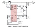
I noticed there is one application note for the minimum feature that replaced the N-CH with a Diode and create a non-synchronous converter.

This is something I could try and it should rule out shoot-through current?
There is no comment or notes how to select this diode though

- - - Updated - - -

Attached:
minimumapp.jpg
 

That smoking was due to dead bits? a 10E resistor with a reverse schottky across it - gives you that fraction more dead time and less RFI ...

too much RFI = mis-performing chip ...
 
Sounds like switching losses are the likely culprit. There are several components to switching loss worth considering.
1. Cross conduction. Obviously this is the most important one to rule out first. Should be ZERO.
2. Vds/Ids overlap. Can be approximated pretty easily. Make sure you use the equations for an inductive load, not a resistive one.
3. Reverse recovery. Actually can be considered a form of Vds/Ids overlap, but adds more complexity to the calculation. Keep in mind that most of the dissipation caused by reverse recovery occurs in the forward FET (the PMOS in your case), rather than the sync FET which actually contains the recovering diode.
4. Losses due to capacitance at the switch node.
Usually you get switching losses only from the hard turn-on of your forward FET (if the inductor ripple current is high enough such that the inductor current is negative before the sync FET turns off, then it's actually possible to get no switching losses...).

This nice article goes through an example step by step. But to get accurate calculations for a synchronous converter, there are a bunch of steps. I usually make excel spreadsheets for this purpose, and there are usually a couple dozen parameters that get factored in.

Of course it could also be a poor layout or something wonky with the controller. Oscilloscope traces would say for sure. I would definitely look into simulating the circuit with LTspice, if you haven't already. They have premade demo simulations for practically every chip they make.
 
Last edited:
Of course it could also be a poor layout or something wonky with the controller. Oscilloscope traces would say for sure. I would definitely look into simulating the circuit with LTspice, if you haven't already. They have premade demo simulations for practically every chip they make.

Thanks for the responses, all.

Unfortunately there is no LTC4011 model for LTspice or demo sim.

I've tried to make a few oscilloscope measurements but the circuit can only be powered for 10-15 seconds before it overheats, which makes actual measurements difficult. I did manage to get a good capture of the switching node voltage on the inductor.
DSC_1312.JPG
Vin = 24V
Vout ~14.8V (battery)
Iout ~2.5A

From the inductive switching equation, this gives me what I need except for Tsw and I'm not quite sure how to measure that without being able to scope the current.

I guess I had thought a chip like LTC4011 would be fairly easy to select compatible switching FETs for a given application without multiple design iterations. I'm not terribly concerned about fine optimization of part cost or board space, I just need to select some FETs that work well and don't get too hot, even if they are 2-3x overkill. My question mostly is where did I go wrong in selecting these specific FETs? Gate charge too much for higher frequency converter? What specifically should I look for in a FET that reduces switching losses?
 

Large fets, & higher voltage fets have slower internal diodes - which lead to switching loss - so choose fets with just enough volt rating and just big enough ( or low enough Rds-ON ) to do the job

If you damage them when soldering - you will have issues - this is more common than you think - as is static damage during handling - which also leads to headaches ...

- - - Updated - - -

p.s. put a schottky across the active fets ( lower ) too - this always helps ...

- - - Updated - - -

p.p.s. that Vds waveform should be square - either the fets or the IC are soft ... or both ...
 
Hi, I have worked on several LT ICs, and to me the problem you are encountering may be related, as Easy peasy already told, to the switching specs of your si7145dp MOSFET. Qg on this fet is 150nC at 5V approx, the previous fet you were using (FDD6637) had a Qg of 25nC.

On the LTC4011 datasheet, page 18, you will find a formula to calculate the power dissipation of the IC. If you calculate it with the value of your previous mosfets, you will find something around 0.9W.

With your "new" fets, you should find something like 2.7W. This IC heats up at 38°C/W, so 2.7W seems a lot. My guess is that the IC doesn't manage to give enough power to drive correctly your fets, and drive them too low, which make them heat a lot.

You should give it a try by only changing your PMOS to the former one.

You can also try to power the INTVdd pin with an external power supply (no more than 5V), I know it is possible on the LTC4020, I don't know for the LTC4011.
 

Large fets, & higher voltage fets have slower internal diodes - which lead to switching loss - so choose fets with just enough volt rating and just big enough ( or low enough Rds-ON ) to do the job

If you damage them when soldering - you will have issues - this is more common than you think - as is static damage during handling - which also leads to headaches ...

- - - Updated - - -

p.s. put a schottky across the active fets ( lower ) too - this always helps ...

- - - Updated - - -

p.p.s. that Vds waveform should be square - either the fets or the IC are soft ... or both ...

Thanks EP
I think primarily it is only the P-FET getting too hot (hard to tell, but the P-FET gets hot first) so I ordered some different P-FETs to try with lower Qg.
SI7143DP-T1-GE3
30V, 35A
rds-on = 10mR
Qg-max = 37nC
Rja = 30 C/W

Also SQJ443EP
40V, 40A
rds-on = 29mR
Qg-max = 57nC
Rja = 65 C/W

I am able to run a full charging cycle now without fear of burning up the FETs but they still get hotter than comfortable. About as bad as the "old" P-FET FDD6637 which had Rds-on of 11.6mR, Qg of 63nC and 96 C/W heating.


Hi, I have worked on several LT ICs, and to me the problem you are encountering may be related, as Easy peasy already told, to the switching specs of your si7145dp MOSFET. Qg on this fet is 150nC at 5V approx, the previous fet you were using (FDD6637) had a Qg of 25nC.

On the LTC4011 datasheet, page 18, you will find a formula to calculate the power dissipation of the IC. If you calculate it with the value of your previous mosfets, you will find something around 0.9W.

With your "new" fets, you should find something like 2.7W. This IC heats up at 38°C/W, so 2.7W seems a lot. My guess is that the IC doesn't manage to give enough power to drive correctly your fets, and drive them too low, which make them heat a lot.

You should give it a try by only changing your PMOS to the former one.

You can also try to power the INTVdd pin with an external power supply (no more than 5V), I know it is possible on the LTC4020, I don't know for the LTC4011.

lipitimisieu,
The 4011 has this in the datasheet:
INTVDD (Pin 14):Internal 5V Regulator Output. This pin provides a means of bypassing the internal 5V regulator used to power the BGATE output driver. Typically, power should not be drawn from this pin by the application circuit. Refer to the Application Information section for additional details.

The BGATE pin drives the N-ch, but the TGATE pin drives the P-ch so it seems adding an external 5V source will only help drive the NMOS?

Here are the switching specs of the LTC4011 if that is helpful:
sw_specs.jpg

I noticed this before but did not expect it to be a problem - why is the TGATE output low (VCC-Tgate) typical about 5V?
So Vgs of the PMOS is -5V in my case instead of -10V or more
I thought the advantage of using a P-CH FET on the high side (less efficient) was that the driving circuit was easier (no bootstrap)? I did use logic-level P-CH FETs (low RDS at Vgs = -4.5V) but I'm just curious.

Now that it is stable enough to run longer, I was able to scope the inductor and gates:
DSC_1332.jpg
SW-node (Vds of N-CH FET)

DSC_1338.jpg
Both Gates

This is with P-CH Si7143DP (Qg = 37nC max)
And N-CH SiR422DP (Qg = 25nC max)


lipitimisieu,
Can you tell me how you found 2.7W from the FET specs and LTC4011 info? If I can calc this for various FETs I can search for something better suited. I can easily increase package/PCB size for this design, is that the best way to increase efficiency?

- - - Updated - - -

EP,
I've just tried adding B360A-13-F (60V 3A) Schottky diodes on both FETs, heating is still too much but rise and fall times seem slightly lower
(maybe 5-10ns lower on N-ch VDS)

Any recommendations for other P-FETs to try? SO-8 PowerPAK preferred or I can try to make a new board with larger footprints? Smaller footprints?

For comparison, the DC674B demo board operates at 2A (up to 10-cell, same as my application) and is using SuperSOT-6 (smaller) package FETs
P-Fet:
FDC658AP
Rds-on = 75mR
Qg = 8.1nC max
Rja = 78 C/W


I'm only trying to squeak 2.5A, maybe 3A if I can out of this design. Should I be using something with extremely low Qg like the above to reduce switching loss?
 

The rise and fall times are too slow - this indicates the chip cannot drive the fets effectively - either the fets are static damaged or just too big ( Cgs and Cdg ) and the total gate charge needed to get them turned on hard is just too much for the chip to supply in ~30nS

What sort of power is the IC targeted at?

for 1W dissipation in a mosfet you need at least 20mm x 20mm on a pcb with no air flow - ideally 2 Oz
 
Ben,

Here is the part of the datasheet allowing you to calculate the power dissipation of the chip:
LTC4011_powerdissip.png

With the last mosfet you used:
Pd = 24V(9mA + 615k(37nC +25nC)) = 1.13W

1.13W * 38°C/W = 43°C temp increase on the LTC4011, but if it has troubles driving the fets, it also increases the switching losses of your fets.

If the gate charge of the PMOS is included in this formula, it is probably because the IC is providing power to drive this gate, thus the gate charge of the PMOS has the same importance as the gate charge of the NMOS. We can see it in your measure, the PMOS has a greater gate charge than the NMOS, and is driven slower. Both are too slow and creating important switching losses.

In the demo board, the mosfets used by Linear are around 5 to 10nC Qg each if I remember well, wich gives a total of 15nC instead of 37 + 25 = 62nC in your case.

To me your options are:
- to use mosfets with lower Qg (probably at the expense of a greater Rdson, but the switching loss are probably predominant here)
- to use external power for INTVCC
 
To me your options are:
- to use mosfets with lower Qg (probably at the expense of a greater Rdson, but the switching loss are probably predominant here)
- to use external power for INTVCC

Thanks, it is all making much more sense now, the power dissipation in the MOSFETs needs to be a trade-off between rds-on losses and switching losses. This converter is higher frequency than my other synchronous converter (LTC4020 at f=200kHz) so gate charge must be a lot smaller.

The first option will be best, but the question is what is the best way to select a lower Qg FET without too much rds-on losses?


For example I found the FDS9400A P-ch FET in SO-8 package.
Rds-on = 200mR @ 4.5V
Qg-max = 3.5nC

Or the DMP3056LSS
Rds-on = 65mR @ 4.5V
Qg-max = 6.8nC

Would either of these be more suitable for a 2.5A buck converter at ~400-500kHz?

Thanks
 

My advice would be to calculate the power losses with each MOSFET, and compare the result. Use an excel sheet with each MOSFET parameters, so you can easily add new mosfets.

For the power losses in your MOSFET, you can use this document: https://www.ti.com/lit/an/slyt664/slyt664.pdf

You can also add to your document the drive losses of the LTC4011 (the formula is in my previous post).

This P-MOS could also be interesting for your application:

STL6P3LLH6
Total Gate charge : 12nC
38mOhms @Vgs = 4.5V
https://www.mouser.fr/datasheet/2/389/stl6p3llh6-956152.pdf

But as I said, you must calculate the losses in your case in order to pick the most suitable one.
 

I have ordered a few different FETs with more similar characteristics to the demo board (capable of 2A)

I have these installed right now:
P-CH: DMP3056LSS-13
"30V, 7.1A"
65mOhms @ Vgs = 4.5V
6.8nC @ Vgs = 4.5V

N-CH: STS10N3LH5
"30V, 10A"
28mOhm @ Vgs = 4.5V
1.7nC @ Vgs = 4.5V

The rise and fall time of the gates is still the same. About 88 to 105ns and they look identical as before.

These are slightly cooler when running but still too hot to hold you finger on the FETs for long.

With 1.7nC and 6.8nC gates, the chip should be able to drive these gates hard and get fast turn on and off times, right? 30ns would be typical?

I'm using a static mat and static tweezers/tools for assembly but maybe the chips are damaged from trying to drive the large FETs?
 

Is your choke heating your fets? - it may well be that the IC is damaged and can't drive them properly - I would expect <50nS rise and fall times ...
 

Just replaced with a new IC, same behavior.

I just tried turning on the circuit while cool and touching the choke and FETs. The FETs are getting hot first, the choke stays cool until the FETs spread heat to the choke. It is definitely the P-FET heating the fastest. It gets hot in about 10 seconds.

FETs reach about 60C, maybe slightly more. With a heatsink attached to the plastic case, the heatsinks gets to 50C so it is not helping very much.

Gates here, same as before (Ch1 = B-gate, Ch2 = T-gate)
DSC_1391.jpg
 

Status
Not open for further replies.

Similar threads

Part and Inventory Search

Welcome to EDABoard.com

Sponsor

Back
Top