Continue to Site

Welcome to EDAboard.com

Welcome to our site! EDAboard.com is an international Electronics Discussion Forum focused on EDA software, circuits, schematics, books, theory, papers, asic, pld, 8051, DSP, Network, RF, Analog Design, PCB, Service Manuals... and a whole lot more! To participate you need to register. Registration is free. Click here to register now.

switching PNP transistor from forward active to saturation states

Status
Not open for further replies.

yefj

Advanced Member level 5
Joined
Sep 12, 2019
Messages
1,505
Helped
1
Reputation
2
Reaction score
5
Trophy points
38
Activity points
9,114
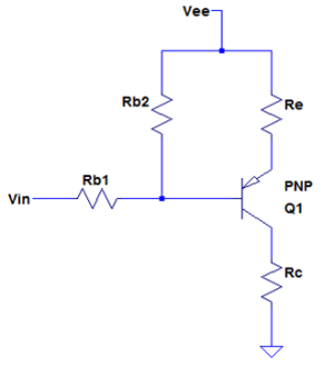
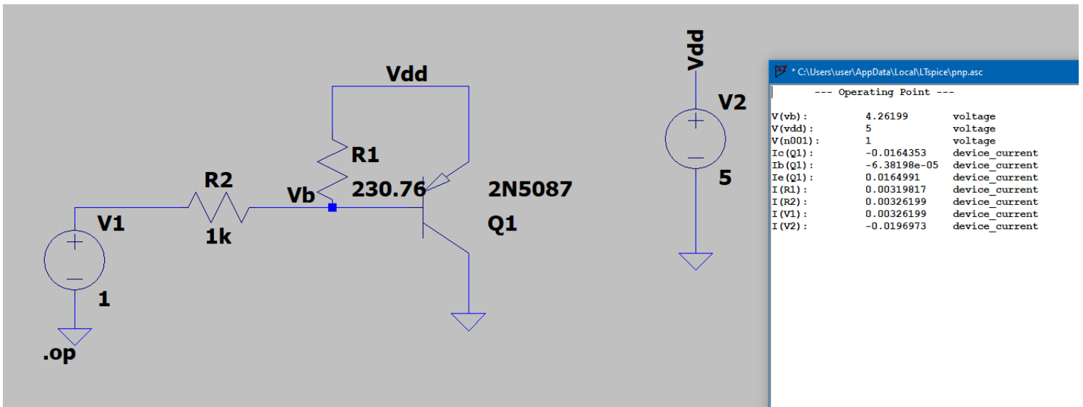
Hello, i have a PNP 2N5087 component which is connected as shown bellow.
for forward active PNP we need the Emitter-base forward biased and base-collector reversed biased.
(emitter)P-N(base) needs to be V_E>V_B to forward biased.
(base)N-P(collector) reversed biased V_base>V_collector.
The base is a voltage divider between V1 and VDD.
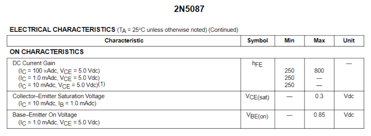
given the datasheet bellow Vbe=0.85 .
but its wrong it should be Veb=0.85 for active region.
i know that the difference between active and saturation is the Vce voltage drop.

how do i put in saturated region my PNP transistor?
should i change my circuit to be able to change the bias from forward active to saturared?
Thanks.
https://pdf1.alldatasheet.com/datasheet-pdf/view/11478/ONSEMI/2N5087.html
1680883462731.png


1680883500563.png
 

You surely noticed that all datasheet voltage and current values have positive sign, although they should be negative according to your assumption. Simply consider that the datasheet uses absolute values, a matter of convention.

You can add a series resistor in collector line, increase it until you observe saturation, e.g. 300 ohms.
 

Hello, two resistors were added to the collector and emmiter as shown bellow.
I know that Ic=(beta+1)I_b (in forward active state) beta=hfe
but i dont know if my transistor is in the active state.
its like what came first the egg or the chicken:)riddle.
I know its an itterative thing.hfe=beta is a range of numbers.
How do i calculate the biasing in this situations?(given that i am not sure what state i am in)
in order to know the Ve and Vc mathematically.
Thanks.

1680888822018.png
 

Bias calculators :


Regards, Dana.
 

Hello ,I have written the equation bellow.
but i dont have the HFE.
What could be done to overcome this obsticle?
Is there some thing i could use in the data sheet?
Thanks.

Vdd-R3*(hfe+1)*ib-0.65+R2*ib=V1
1680899722988.png
 

If you can apply Thevenin rules for attenuation, Consider Base input impedance is Rin= hFE*(Re+rbe) with hFE = 200 and Re=100 then Rin > 20k which in parallel with source R's means hFE and base current can be neglected here.

The 2N5089 was a popular low noise high hFE audio PNP, identical to the 2N5088 NPN half a century ago.

For Saturation zone in Red
1680916531557.png

Vce|< 2V as the start of saturation where hFE begins to reduce quickly towards Ic/Ib=10 at low current but at high current the threshold reduces towards |Vce|<0.7 where Vbc is forward conducting.

However datasheets will standardize Vce(sat)= xxx max @ Ic with a Ic/Ib = fixed ratio usually <10% of hFE max. or default = 10

1680916741912.png
 
Last edited:

Hello ,from figure 9 of the data sheet if we take the Ic=20mA so Ib=2mA point in Saturation state our Vce=0.1V and Vbe_sat =0.8V given 20mA.
am i correct?

Assuming i am correct i have a problem with the KCL in the base junction.
I know the Ib=2mA and i have voltage divider.
how do i combine the two to know what current flows at R1?
Thanks


1680967738597.png


1680967714007.png
 

Review how to compute Thevenin node voltage at the base with transistor removed.
The base input R is unknown due since Vbe is unknown but we will see it is not 0.8V.

The Thevenin base voltage Vth= 4.25 V, Rth = 187 = 230 || 1k
leaving only 0.75V = |Vbe| + Ie*Re
Your assumption was |Vbe| = 0.8 V is not possible The base current is uncertain since the pullup resistor is far too small and ought to be in the 10x Re range because now the base-emitter resistance will be significant and also in this range< 100 ohms so bias is more predictable when the bias resistors are much bigger than the base-emitter.

We see below when Ic = 1mA, Vbe max is = 0,65 Vand this drops <= 6.25V as Vce rises to 1V where hFE will be higher.

So we can say Ie max= 0.75- 0.625 / 100 ohm= 125 mV/100 = 1.25 mA @ 25'C

Any questions?

1680977010606.png


For R1=230, R2 = 1k and Vcc= 5V , Vin =1V Bias current is 4V/ 1230 ohms = 3.25 mA is probably more than your collector current.
If you wanted Ic = 20mA then you would increase R1 to get Ve= 5V-20mA*100=3V across emitter R then drop the Vb by 0.7 (est.) to create Vth = 2.3V at the base. then you would expect Vce = 1V.

Then I would expect R1 to be around 2k2. I'll let you prove me right or wrong.
 
Last edited:

Falstad's interactive simulator displays transistor specs during a run, including whether saturated/ cutoff/ fwd active. Hover the cursor on it as in screenshot below. Notice it tells volt levels. Currently in saturation. Gain is set to 800 (default is 100).

Free to download and use:

Falstad.com/circuit

PNP specs display in Falstad's simulator.png
 

To meet the saturation condition is a very simple task: You only need to know the collector resistance Rc and the switching signal Vs.
* Saturation meens:
The base-collector junction is biased in forward mode - therefore, the collector current must be be selected so that the voltage drop across Rc is large enough to make the potential at the collector lower (npn case) or larger (pnp case) than the base potential.
Then, as the next step, you can find the base resistor Rb using the voltage divider rule (between the base resistor Rb and the base-emitter juntion (use Vbe=0.7 volts): Rb=(Vs-Vbe)/Ib.
For the base current Ib you can assume Ib=Ic/10 (no need to know the factor beta=hfe for the linear case).
 

Here , making the bias more useful with near unity bipolar output gain due to 50 ohm gen. attenuation.

Then change to std bias with R ratios to get +/-1V swing on both outputs leaving 0.3V margin to each rail. using base resistors about <=100 x Rc

Then combine plots & choose property manual scale typing 750 mV/div and slide offset of plot left to 0V at the bottom then undock and stretch over schematic.

There is an interactive switch after the AC coupled sig. gen with added 50 Ohm and the gen. set to 1V pk (2Vpp) thus a total differential swing on the output near 4Vpp but actually each is only 1.92 Vpp.

Note the effect of hFE on the stable H bias a very wide range on the slider option. Yet not as stable as with negative feedback.

When you want to saturate the output as a switch then you increase the input but you must change the bias to reduce hFE or Ic/Ib ratio towards but does not have to be = 10..

1681052541563.png


Any questions?
 
Last edited:
  • Like
Reactions: BradtheRad

    FvM

    Points: 2
    Helpful Answer Positive Rating
forward active state ?
Generally, Forward Active is defined as |Vce|>2 approximately, which is useful for designs that depend on more constant hFE.

But as you can see the corner voltage drops with the current in the Saturation Region shown below for NPN.
1681072943078.png

When we use saturation as a binary or logic level, you don't want to choose just the threshold of saturation, but rather full saturation considering all tolerances at or below the logic level specified.

Notice I used |Vce| so either PNP or NPN applies.

Otherwise Vce for PNP looks like this.
1681073126737.png

--- Updated ---

Saturation is also the region where Vce transitions from a high impedance current-source into a resistive inverting switch. Where Rce=Vce(sat)/Ic is low for PN2222A around 1 Ohm but rather high for the high beta , low noise 2N5087 not famous for being used yet can be as low current switches and are efficient due to the high hFE. if you use 3% of max hFE rather than 10% or Ic/Ib=20.

. Vce when hFE is known to drop rapidly as a % of max hFE.
1681075015690.png
 
Last edited:

Hello In the datasheet we have Vbe_Sat and and Vce_sat plots shown bellow.
Why picking 20mA values Vbe_Sat and and Vce_sat are wrong?
The plot says it could be in saturation with this conditions ,why its wrong to see things like that?
Thanks.

1681213135731.png
 

Hello Dana,So if nothing wrong then i chose to bias my PNP with Ic=20mA so Ib=2mA Vce=0.1V and Vbe_sat =0.8V as shown in the plot bellow.why its not possible to create such conditions from my circuit shown bellow?(disregard hte values of the resistors)

1681215203174.png


1681215308064.png
 

There is nothing wrong with the graph.....

You are being shown, for Ib = Ic/10 and a range of Ic what Vce(sat)
and Vbe looks like.


Regards, Dana.
 

Hello In the datasheet we have Vbe_Sat and and Vce_sat plots shown bellow.
Why picking 20mA values Vbe_Sat and and Vce_sat are wrong?
The plot says it could be in saturation with this conditions ,why its wrong to see things like that?
Thanks.

View attachment 182251
The plots are correct only if the conditions are true. Ic/Ib=10
In your initial question, This was not true as very little of the bias current went into the base so the Vbe condition was not satisfied to achieve Ic=20 mA.

Please review my answers and ask a better question.
 
Hello I have tried to use the data sheet and math of the daa from the data sheet and i got it to active mode unfortunetly.
I need some how to recreate the plots of VCE SAT and Vbe SAT.
how do i create a plot with a current and x axes knowing that these plot put my pnp in Saturation?
Thanks.


1681229354771.png

--- Updated ---

UPDATE:
I managed to get it into saturation .
but i want to recreate the data sheet plots in LTSPICE.
How can i sweep my circuit to do such plots?
Thanks.
1681233157197.png
1681233051388.png
 
Last edited:

A simulator as LTspice has all means to setup a test with the given conditions, a) Ic/Ib = 10, b) Vce = 1.0 V. Repeatedly posting the same simulation circuit and stating that it doesn't achieve the intended operation point is just boring. Think again!
 
Status
Not open for further replies.

Similar threads

Part and Inventory Search

Welcome to EDABoard.com

Sponsor

Back
Top