navbp
Junior Member level 1

Hello All,
I need help to develop a PCB for an embedded system which also supports High current.
Max. Voltage on the PCB : 56V
Max. Current on two traces: 150A for 10s, Nominal current of 120A for few mins.
Number of layers possible : 6 to 8 layers
5 MOSFETs in parallel (2mOhm Rdson)
Thermal management : Cooling not possible / MOSFETs Without heatsinks
PCB will have one or two components which are BGA package.
MOSFETs have to be mounted on the PCB too which carry such high currents.
As BGA package components are to be used, the outer layer copper thickness should be 1 Oz. and Inner layer shall carry high currents which can be of 2Oz or 3Oz thickness.
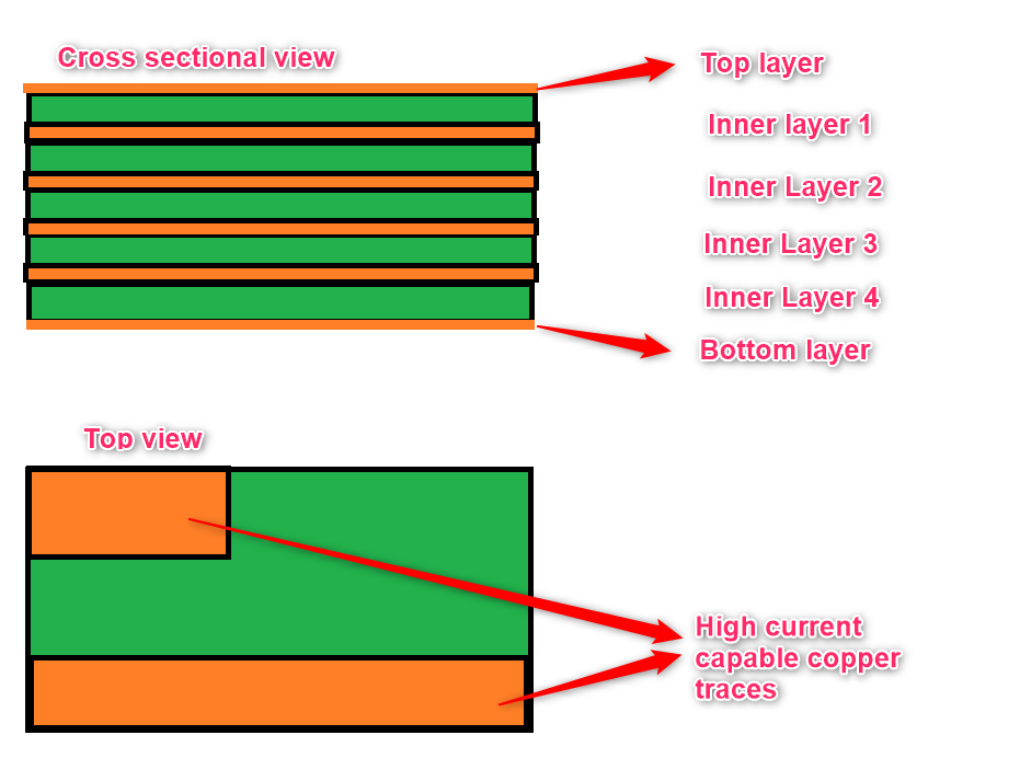
As the current is high, I am planning to use traces on all layers in parallel with vias to handle this current.
i.e., The copper traces shown in the top view will be available in every layer of the PCB and they are all connected using vias.
Outer layers : 1Oz
Inner layers : 2Oz or 3Oz possible
An image of the PCB planned is attached.
My queries / concerns:
1. Is 2Oz copper thickness for inner layers enough to handle such a high current? Or do we need to go for 3 Oz copper thickness?
2. Due to high current and MOSFETs which are carrying this current, the PCB gets hot. It is not easy to get the heat out of inner layers. Any suggestions here?
3. What is the suitable stackup for this application? Is the stackup mentioned below fine?
Top : Signal layer / Components
Inner1: Signal
Inner2: Power
Inner3: GND
Inner4: Signal
Bottom: Signal / Components
4. Is it fine to route signal traces through the inner layers as the copper thickness of inner layers is higher?
5. What should be size of the vias which has to be used?
Thank you in advance.
Regards,
Naveen.
Last edited by a moderator:
