BubenFFT
Newbie level 5

Hi,
I have an RF PCB with CPWG that changes it's sizes.

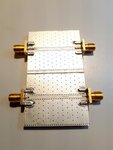
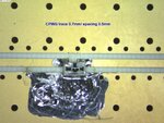
See the attached photo. I wanted to measure this board with a VNA. I first attached SMA connectors with long (4mm) central pins (the top PCB on the photo). The RL was not that great. I then thought that it is affected by stray capacitance of the very long pin and solder under it. I cut central pins to approx. 1mm and soldered them to another board (the bottom PCB on the photo). I see on VNA that RL is greatly improve.

The green trace is for the SMA connectors with long central pins, the blue trace is for the SMA connectors with trimmed central pins. What puzzles me is that according to Smith chart, the long central pins and solder under them introduces more stray inductance rather than stray capacitance. I expected stray capacitance. Does anyone know why is that?
Thanks
I have an RF PCB with CPWG that changes it's sizes.

See the attached photo. I wanted to measure this board with a VNA. I first attached SMA connectors with long (4mm) central pins (the top PCB on the photo). The RL was not that great. I then thought that it is affected by stray capacitance of the very long pin and solder under it. I cut central pins to approx. 1mm and soldered them to another board (the bottom PCB on the photo). I see on VNA that RL is greatly improve.

The green trace is for the SMA connectors with long central pins, the blue trace is for the SMA connectors with trimmed central pins. What puzzles me is that according to Smith chart, the long central pins and solder under them introduces more stray inductance rather than stray capacitance. I expected stray capacitance. Does anyone know why is that?
Thanks


