surendran_raj
Junior Member level 2

Hi,
I need some clarification about ADC in injected conversion method. I am using STM32F103C8 controller I configure TIM1 in center align mode 1 to trigger the ADC in injected mode. i worked well and tried to check the ADC in injected mode by making pin PB1 to high and making it low after reading data in ADC->DR register in ADC1_2_IRQHandler(). But i need to trigger and read the ADC data at the center of the ON time pulse of TIM1. can anyone help me to get it?. i have attached my code.
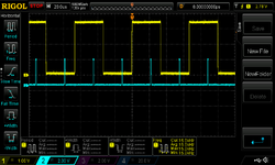
When TIM1->RCR = 0; ADC is triggered at both ON and OFF time of PWM(TIM1).
channel 1 - TIM1 PWM (15KHz in center align mode 1).
channel 2 - pin PB1 is made HIGH and made it LOW after reading the data in ADC->DR in ADC1_2_IRQHandler() to know where the ADC is triggered.

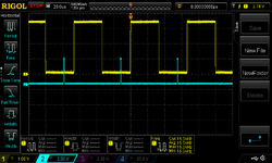
When TIM1->RCR = 1; ADC is triggered at the OFF time of PWM(TIM1).
channel 1 - TIM1 PWM (15KHz in center align mode 1).
channel 2 - pin PB1 is made HIGH and made it LOW after reading the data in ADC->DR in ADC1_2_IRQHandler() to know where the ADC is triggered.

I need to trigger and read the ADC value at the center of the ON time pulse. can anyone help me to solve it.
I need some clarification about ADC in injected conversion method. I am using STM32F103C8 controller I configure TIM1 in center align mode 1 to trigger the ADC in injected mode. i worked well and tried to check the ADC in injected mode by making pin PB1 to high and making it low after reading data in ADC->DR register in ADC1_2_IRQHandler(). But i need to trigger and read the ADC data at the center of the ON time pulse of TIM1. can anyone help me to get it?. i have attached my code.
Code:
#include<stm32f10x.h>
int read_A7=0,read_B0,read2=0;
int  counter=0;

void TIM1_init(void)
{
    RCC->APB2ENR |= RCC_APB2ENR_TIM1EN;

    TIM1->PSC =0;
    TIM1->ARR = 2400;
    TIM1->CCR1 = 1200;

    TIM1->CCMR2  |=TIM_CCMR2_OC4M_1|TIM_CCMR2_OC4M_2|TIM_CCMR2_OC4PE;
    TIM1->CCMR2  |=TIM_CCMR2_OC3M_1|TIM_CCMR2_OC3M_2|TIM_CCMR2_OC3PE;
    TIM1->CCMR1  |=TIM_CCMR1_OC2M_1|TIM_CCMR1_OC2M_2|TIM_CCMR1_OC2PE;
    TIM1->CCMR1  |=TIM_CCMR1_OC1M_1|TIM_CCMR1_OC1M_2|TIM_CCMR1_OC1PE;

    TIM1->CCER   |=TIM_CCER_CC4E|TIM_CCER_CC3E|TIM_CCER_CC2E | TIM_CCER_CC1E;
    TIM1->BDTR   |=TIM_BDTR_MOE;
    TIM1->CR1    |=TIM_CR1_CMS_0|TIM_CR1_CEN;
    TIM1->EGR    |=TIM_EGR_UG;

    TIM1->CR2 &= ~ TIM_CR2_MMS;
    TIM1->CR2    |= TIM_CR2_MMS_1;
    TIM1->RCR = 1;
    TIM1->DIER = TIM_DIER_UIE;

    NVIC_EnableIRQ(TIM1_UP_IRQn);

}
void ADC2_init(void)
{
    RCC->APB2ENR |=RCC_APB2ENR_ADC2EN;
    RCC->CFGR |=RCC_CFGR_ADCPRE_DIV6;

    ADC2->CR2 |=ADC_CR2_JEXTTRIG;
    ADC2->CR2 &=~(ADC_CR2_JEXTSEL_0|ADC_CR2_JEXTSEL_1|ADC_CR2_JEXTSEL_2);
    ADC2->JSQR |= (1<<21);
    ADC2->JSQR |= ((1<<17)|(1<<16)|(1<<15)|(1<<13)|(1<<6)|(1<<5));
    ADC2->CR2 |= ADC_CR2_ADON;
    ADC2->CR1 &=~ADC_CR1_JAUTO;
    ADC2->CR1|=(ADC_CR1_SCAN |ADC_CR1_JEOCIE);
    ADC2->CR2 |=(ADC_CR2_JSWSTART);

    NVIC_EnableIRQ(ADC1_2_IRQn);


}
int main(void)
{
    RCC->APB2ENR |= RCC_APB2ENR_IOPAEN | RCC_APB2ENR_IOPBEN | RCC_APB2ENR_AFIOEN;
    GPIOA->CRH = 0x00000BBB;
    GPIOA->CRL = 0x00000000;

    GPIOB->CRL = 0x00000030;
    TIM1_init();
    ADC2_init();

    while(1)
    {

    }
}

void TIM1_UP_IRQHandler(void)
{
    if(TIM1->SR & TIM_SR_UIF)
    {
        TIM1->SR&=~TIM_SR_UIF;

    }
}

void ADC1_2_IRQHandler(void)
{
    if(ADC2->SR | ADC_SR_JEOC)
    {

        ADC2->SR &=~ (ADC_SR_JSTRT | ADC_SR_JEOC);

        GPIOB->ODR |=1<<1;
        read2 = ADC2->JDR1;
        read_B0 = ADC2->JDR2;
        read_A7 = ADC2->JDR3;
        GPIOB->BRR = 1<<1;

 }

}
When TIM1->RCR = 0; ADC is triggered at both ON and OFF time of PWM(TIM1).
channel 1 - TIM1 PWM (15KHz in center align mode 1).
channel 2 - pin PB1 is made HIGH and made it LOW after reading the data in ADC->DR in ADC1_2_IRQHandler() to know where the ADC is triggered.
When TIM1->RCR = 1; ADC is triggered at the OFF time of PWM(TIM1).
channel 1 - TIM1 PWM (15KHz in center align mode 1).
channel 2 - pin PB1 is made HIGH and made it LOW after reading the data in ADC->DR in ADC1_2_IRQHandler() to know where the ADC is triggered.
I need to trigger and read the ADC value at the center of the ON time pulse. can anyone help me to solve it.


