Continue to Site

Welcome to EDAboard.com

Welcome to our site! EDAboard.com is an international Electronics Discussion Forum focused on EDA software, circuits, schematics, books, theory, papers, asic, pld, 8051, DSP, Network, RF, Analog Design, PCB, Service Manuals... and a whole lot more! To participate you need to register. Registration is free. Click here to register now.

Startup Circuit Issue

nahid99

Newbie level 4
Newbie level 4
Joined
Mar 6, 2024
Messages
7
Helped
0
Reputation
0
Reaction score
2
Trophy points
3
Activity points
65
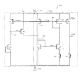
I designed a supply independent bias circuit commonly known as beta multiplier current reference. So, i used a start-up circuit to this circuit. While the transient simulation i plot the startup current, it rise up then backwards. I don't understand why it goes up to the negative side. Can anyone help me that what is the issue. Also, can anyone suggest that how to choose proper sizing for the startup circuit. Thanks

1726496451505.png

1726496485877.png
 
dV/dt against a bunch of "off" (w/ Cxx everywhere except the load). What else could happen below Vdd-Vss=VT?

Think about how / where to suppress outcomes as you will never get rid of all of it.
 
Hi @nahid99
From the drawing provided it seems like your startup circuit doesn't even work (just look at the order of currents, it is in nanoamperes).
One of the ways you can verify that is by setting the initial condition in Spectre to force your Vbiasp=0 and Vbiasn=VDD. Your circuit most likely will stay locked in this condition, because your startup is enabling MN3 hence shorting Vbiasp and Vbiasn which wouldn't force the transistors in beta multiplier to start conducting.

The purpose of the startup circuit is to let the currents flowing your circuit at the initial condition -> hence we need to design a circuit that in your case will pull down Vbiasp to 0 and Vbiasn to VDD and disconnect when the currents will start flowing.

I could recommend using some circuit like this (attached). The key point here is that the diode-connected device (N3 on the drawing) has to be quite small (and probably long) so that the P4 should give more current after the currents will start flowing and hence will disconnect the P3 from the main circuit.

Hopefully, that helps.
 

Attachments

  • 1726497579393.png
    1726497579393.png
    41.9 KB · Views: 13
Hi @nahid99
From the drawing provided it seems like your startup circuit doesn't even work (just look at the order of currents, it is in nanoamperes).
One of the ways you can verify that is by setting the initial condition in Spectre to force your Vbiasp=0 and Vbiasn=VDD. Your circuit most likely will stay locked in this condition, because your startup is enabling MN3 hence shorting Vbiasp and Vbiasn which wouldn't force the transistors in beta multiplier to start conducting.

The purpose of the startup circuit is to let the currents flowing your circuit at the initial condition -> hence we need to design a circuit that in your case will pull down Vbiasp to 0 and Vbiasn to VDD and disconnect when the currents will start flowing.

I could recommend using some circuit like this (attached). The key point here is that the diode-connected device (N3 on the drawing) has to be quite small (and probably long) so that the P4 should give more current after the currents will start flowing and hence will disconnect the P3 from the main circuit.

Hopefully, that helps.
Hi, @sidun.av
Thanks for your valuable reply, I modified the schematic & update the start-up what you suggested. I get the output bellow, could you please check? Whether is working properly or not? I am waiting for your valuable review, thanks.

1726681211985.png
 
I cannot say that your start-up is working or not to be honest...
1. It's very hard to see the current on your graph. You have a peak current of 240mA (at VDD = 0V) at the beginning of your sim, which doesn't make any sense and looks like an artefact. Try to change your analysis precision to conservative preset, to avoid this.
Basically, you should see a peak of a few uA through your start-up circuit for a short period of time, somewhere on a rising edge of VDD, and then quick drop of this current to 0 (when your core turns on).

2. As I previously mentioned, in your transient analysis you need to force Vbiasp to be VDD and your Vbiasn to be VSS at the beginning in order to see how your start-up circuit will deal with this situation.
In your ADEL go to Simulation -> Convergence Aids -> Initial condition and set Vbias nodes to mentioned voltages. After that you can plot Vbiasp, Vbiasn and your start-up current (i.e. ) through NM2 and see how your Vbias voltages will (or will not) go from VDD/VSS to the desired levels. This simulation should give you better understanding how does the start-up circuit works and you will be able to decide optimum W/L values.

3. Once your circuit is running okay, you would need to test it across PVT. In this case, your approach with ramping the VDD will be useful, as transient simulation is more accurate. For such circuits, I am usually having a set of VDD ramps with 10u(fast) and 100u (slow) front reaching nominal VDD +- 10% and also testing this across process corners and MC.

You may also find this useful:
 
Last edited:

LaTeX Commands Quick-Menu:

Similar threads

Part and Inventory Search

Welcome to EDABoard.com

Sponsor

Back
Top