namooon
Newbie

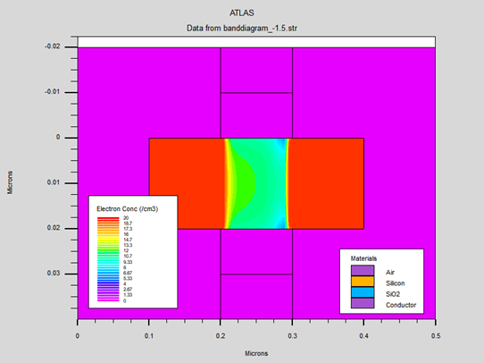
I'm trying to analyze the gidl effect on DG-MOSFET, but the electron concentration on the channel region kept growing while the gate bias is getting bigger to the negative direction.
I think the electron concentration should be lowered as the gate bias is getting bigger to the negative direction.
And I'm guessing error is formed because of the diffusion of the electron from n+doped source to the p-type body region. The gate length is set 100nm, but the diffusion kept seen.
I have been trying to solve this problem, but I couldn't.

this is the electron concentration when the gate voltage is -1.5V, and the drain voltage is 1V.

you can see that as the gate voltage grow from -0.3V to -2.4V, the electron concentration on the channel region get higher.
Can I get some advise for this?
I think the electron concentration should be lowered as the gate bias is getting bigger to the negative direction.
And I'm guessing error is formed because of the diffusion of the electron from n+doped source to the p-type body region. The gate length is set 100nm, but the diffusion kept seen.
I have been trying to solve this problem, but I couldn't.
this is the electron concentration when the gate voltage is -1.5V, and the drain voltage is 1V.
you can see that as the gate voltage grow from -0.3V to -2.4V, the electron concentration on the channel region get higher.
Can I get some advise for this?