Continue to Site

Welcome to EDAboard.com

Welcome to our site! EDAboard.com is an international Electronics Discussion Forum focused on EDA software, circuits, schematics, books, theory, papers, asic, pld, 8051, DSP, Network, RF, Analog Design, PCB, Service Manuals... and a whole lot more! To participate you need to register. Registration is free. Click here to register now.

Software to reverse engineer a PCB

Status
Not open for further replies.

wirewizard

Newbie level 4
Newbie level 4
Joined
Feb 2, 2019
Messages
5
Helped
0
Reputation
0
Reaction score
0
Trophy points
1
Activity points
66
I try to do a reverse engineer a schematic of a faulty board i want to repair (only for private, not commercial). It consist of about 140 parts, a MCU and some other ICs, but also many transistors, diodes and suchs. I've spent many hours to dig into rev-eng and looking for tools to assist in building schematic from netlists, but the only one i found was Target 3001 in Design-Station Edition, which is about 3k€ :-(

Anyone knows any other tools which are able to make a schemtic out of components placed on boards and connected the pads by following the wires and vias? OpenSource or Freeware is highly recommended, since i can't spend much money on this.
 

Someone needs to write an app for this.
Take photo of board, app decodes it and provides you with full schematic, parts list and Gerbers.

Coming soon to an Android or Apple phone near you.

ROFLMAO.

(PCB reverse engineering is a damn site harder than your suggesting - use a pencil, eraser and paper for best results.)
 

I've seen this kind of thing promoted on LinkedIn but
can't remember the name / vendor. If it crosses my
feed again I'll post.
 

If you have Gerber data you can do a fair bit of reverse engineering in the front end programs such as CAM350, this will give you a net-list to check to.
Most people offer a reverse engineering service, we do it for old mil designs etc. where data has been lost etc. If we have a board we will get a PCB manufacturer to probe it and get us a net-list to work to, for checking... Other than that its work, work work.... and if its a multi layer! well it just gets harder, that's why we strive to get a net list...
 

RE-creating this board -if the schematic is available- is much easier.If even the schematic is not available, designing a similar circuit takes lesser time than digging the actual board.
If this board has 4 or more layers, forget about it.. It's almost impossible..
 

No, of course the schematic is not available. Love to see a tool doing all the work, but i'm not lazy. For now, i don't know how, meaning of what to use? Gerber, i think are only usefull for etching and drilling.

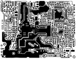
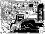
I've already "prepared" the board in question, for heavens sake only a dual layer one, for rev-eng. Removed all parts, inventoried them, remove the silk screen down to blank copper, scanned both sides to achieve a unbended view of the layers. Also postprocessed the images to b/w. A good starting point, i guess :)
Only thing i could do with the image, may be to remove the mass areas which are not connected to any pad or via. But this, i guess, is only for better visualization the rest.

The principle to reverse from board seems to place the images as silk screen layers on top and bottom, then place all the parts (which are in fact only the pads), vias and connectors. Next connect everything by following each lane from pad to pad/via. This should result in a netlist. Target 3001 can do this, even in the free edition. But then some "magic" needs to encode a schematic from this netlist. This little part is what is missing for free and only available by paying thousands of Euros ;-(
 

I presume, even a tool with dedicated reverse engineering functions can't place the schematic symbols in a meaningful pattern, it's up to you to understand the basic circuit operation and arrange the components respectively.

Without a dedicated tool, recreating the schematic isn't much different. I would use pencil and paper in a first step. Sketch the circuit, verify against the PCB netlist, entry into schematic tool.
 

No, you misunderstood me. I don't expect to get a nice layouted schematic. All i want is a plan with ratsnest placed parts which are connected accoring to the netlist.

Pen and Paper?! I don't think you want to do this with this PCB:

b1549218978.31245.jpgb1549218978.31243.jpg
 

Hi,

Pen and Paper?! I don't think you want to do this with this PCB:
No one likes to do it this way...

But do you have any other chance? I don´t see one.

Klaus
 

RE-creating this board -if the schematic is available- is much easier.If even the schematic is not available, designing a similar circuit takes lesser time than digging the actual board.
If this board has 4 or more layers, forget about it.. It's almost impossible..

Not quite impossible, but very very time consuming, including having x-rays done of inner layers, customer had DEEP pockets...

- - - Updated - - -

No, you misunderstood me. I don't expect to get a nice layouted schematic. All i want is a plan with ratsnest placed parts which are connected accoring to the netlist.

Pen and Paper?! I don't think you want to do this with this PCB:

View attachment 151364View attachment 151365

Something this easy I would convert the images to DXF, read them into the CAD package and use them as a guide.

- - - Updated - - -

No, of course the schematic is not available. Love to see a tool doing all the work, but i'm not lazy. For now, i don't know how, meaning of what to use? Gerber, i think are only usefull for etching and drilling.

From Gerber data you can re-create a netlist of the design, most Gerber front end programs let you group pads to create footprints and components so there is quite a lot you can do with Gerber data if you have the tools and the know how.

Creating schematics is a very hands on affair, even if you can back annotate a PCB to a schematic there is still lots of drafting to do.
 
  • Like
Reactions: FvM

    FvM

    Points: 2
    Helpful Answer Positive Rating
Status
Not open for further replies.

Part and Inventory Search

Welcome to EDABoard.com

Sponsor

Back
Top