Continue to Site

Welcome to EDAboard.com

Welcome to our site! EDAboard.com is an international Electronics Discussion Forum focused on EDA software, circuits, schematics, books, theory, papers, asic, pld, 8051, DSP, Network, RF, Analog Design, PCB, Service Manuals... and a whole lot more! To participate you need to register. Registration is free. Click here to register now.

SMPS circuit fault analizing help

Status
Not open for further replies.

Ranbeer Singh

Full Member level 5
Full Member level 5
Joined
Jul 30, 2015
Messages
259
Helped
22
Reputation
44
Reaction score
22
Trophy points
1,298
Location
Faridabad India
Activity points
3,266
Hello,

i want some help regarding to SMPS circuit fault correction. In the PCB circuit i found the driver mosfet ic is damaged (locking physically). I want to know, what other components (like any diode) can be damaged as per this situation.

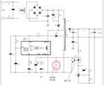
Circuit diagram

Untitled2.png

Thanks in advance.
 

VIPER 20 is an integrated fly back switch, this IC may burn due to its internal circuit problems so no other external components will effect. If the IC is burn badly then surrounding components may distort. For a complete troubleshooting, First check BR1 Bridge rectifier,if BR1 is ok then check D3 and ISO1
No other components failure
 
Although the silicon components are generally more prone to burn, and the electrolytic capacitors are also affected in the event of any overvoltage, I would not rule out the possibility that the transformer if it is not burned, that at least had its properties changed, In the case of overheating of the insulation varnish of the windings; Just a guess.
 

Thank you very much

I will try according your instruction and will reoprt.


Although the silicon components are generally more prone to burn, and the electrolytic capacitors are also affected in the event of any overvoltage, I would not rule out the possibility that the transformer if it is not burned, that at least had its properties changed, In the case of overheating of the insulation varnish of the windings; Just a guess.

Yes you can be right.
 

Hi,

I checked pcb circuit and found a zener diode (do not have any value on it) is connected on opto 817B collector and emitter pin (see attached picture). I checked it with multimeter and found it resistance was 25E in both condition (probe changed).

IC Viper53 datasheet says

COMP pin
"Input of the current mode structure, and output of the internal error amplifier. Allows
the setting of thedynamic characteristic of the converter through an external passive
network. The useful voltage range extends from 0.5V to 4.5V. The Power MOSFET is
always off below 0.5V, and the overload protection is triggered if the voltage exceeds
4.35V. This action is delayed by the timing capacitor connected to the TOVL pin."

and

"The VIPer53 device delivers a constant current of 0.6 mA on the COMP pin,
creating a constant voltage of 0.6V in R5 and a rising slope across C7. This voltage shape,
together with the operating range of 0.5V to 4.5V provides a soft start-up of the converter."

My question is, what is the value of zener diode?
Is it damaged?


SMPS circuit.png
 
Last edited:

Hi,

Schematic symbol is not look like Zener; any way I believe your word.

If the Zener diode reads low resistances in both directions, this is a sign that the diode is shorted. A diode should not measure low resistance in the reverse biased direction. Defected diode will cause the compensation pin voltage always less than 0.5V, so the mosfet will remain off state
Over voltage protection will work if the voltage on the com pin exceeds 4.35V. So the Zener voltage will fall between 9V to 15V
 

So the Zener voltage will fall between 9V to 15V

I am not understanding, if 4.35v is comp pin threshold limit voltage. It's means if limit crosses, over voltage condition will occur and mosfet will be off. I mean the voltage never will above 4.35. So how will we need a much voltage zener diode.
 

Data sheet says
Input of the current mode struct
ure, and output of the intern
al error amplifier. Allows
the setting of thedynamic c
haracteristic of the converter through an external passive
network. The useful voltage range extends fr
om 0.5V to 4.5V. The Power MOSFET is
always off below 0.5V, and the overload prot
ection is triggered if the voltage exceeds
4.35V. This action is delayed by the
timing capacitor connected tothe TOVL pin.

It means if the voltage exceed 4.35V(Due to overload) then only overload protection will work by varying the pulse sequence. If you put 4.35V Zener at that place over load protection should not work

Hope it is clear
 

Status
Not open for further replies.

Similar threads

Part and Inventory Search

Welcome to EDABoard.com

Sponsor

Back
Top