Continue to Site

Welcome to EDAboard.com

Welcome to our site! EDAboard.com is an international Electronics Discussion Forum focused on EDA software, circuits, schematics, books, theory, papers, asic, pld, 8051, DSP, Network, RF, Analog Design, PCB, Service Manuals... and a whole lot more! To participate you need to register. Registration is free. Click here to register now.

Smartphones' Powerbank

Status
Not open for further replies.

Hunter666_444

Newbie level 4
Newbie level 4
Joined
Apr 20, 2019
Messages
7
Helped
0
Reputation
0
Reaction score
0
Trophy points
1
Activity points
65
Hello y'all

I want to make a power-bank PCB and I really can't find any good schematics so please if anyone has any leads and this is my 3rd PCB ever if there is any notes or advice I really appreciate it

Thanks in advance :-D,
 

What do you mean by a good schematic? What is lacking in the schematics that you found online? Can you talk a bit more about that, along with your project requirements?

You would want to see a battery charge controller (for charging the bank) and a boost converter (or a linear regulator for discharging the bank; charging other devices) with simple load protection circuits (diode for reverse polarity protection, for example) in a bare-bones powerbank.
 

Most "Power banks" are nothing more than four NiMH cells in series inside a box. The phone will have some kind of charge regulator inside it so as long as the "power bank" looks like the output of a wall adapter it will work.

Note that many cheap "Power banks" have much smaller capacity than they quote and even have chalk or sand inside them to make them feel as though they contain bigger cells!

Google for "power bank scams" to see what they contain.

Brian.
 

Hi,

Most "Power banks" are nothing more than four NiMH cells in series inside a box.
I'd be surprised.
Usualy they have a USB connector, thus I assume the output voltage needs to be regulated to keep on USB supply standards.
Otherwise one risks overvoltage and damage of a USB device connected to the power bank...or undervoltage causing malfunction.

But I don't know for sure.

Klaus
 

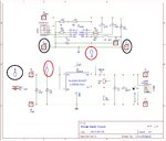
requirements is that the output should be 5v at 1000mA and has an LCD that shows percentage.The schematics I found online are made of 2 parts and I didn't understand them as there is no connection and there is some missing things as I want to make a simulation for the circuit on Proteus I circled what I can't understand,and if you know please give me some clues and after printing the design what should I connect in these nodes ?

Thanks in advance


q1.jpg
 

Hi,


I'd be surprised.
Usualy they have a USB connector, thus I assume the output voltage needs to be regulated to keep on USB supply standards.
Otherwise one risks overvoltage and damage of a USB device connected to the power bank...or undervoltage causing malfunction.

But I don't know for sure.

Klaus

Agreed, I do know that all phones contain some sort of buck-boost converter but I'm not sure if that also extends towards the charging port as a secondary protection feature.

requirements is that the output should be 5v at 1000mA and has an LCD that shows percentage.The schematics I found online are made of 2 parts and I didn't understand them as there is no connection and there is some missing things as I want to make a simulation for the circuit on Proteus I circled what I can't understand,and if you know please give me some clues and after printing the design what should I connect in these nodes ?

Thanks in advance


View attachment 155268

1. The top part of the schematic has a TP4058 linear battery charge controller, so it is obviously meant for charging the bank's cells in a controlled manner. The bottom part of the schematic has a XL6009 boost converter to step-up voltage, so it is obviously meant for discharging the bank's cells (and charging other devices). I assume whoever designed the circuit did it in a modular manner instead of creating a convoluted mess of a circuit.

2. Although there are no "visible" wire connections from one point to another, it doesn't mean that the circuit design is faulty or incomplete. I'm not exactly sure what the proper term is for those input/output ports (or terminals, however it's called), but their function is to act as an "invisible" wire connection from one point in the circuit to another. This function is identified as hierarchical ports in PSpice (PORTLEFT/PORTRIGHT), and INPUT/OUTPUT terminals in Proteus.

Since you referred the schematic from a different source, I'll leave it to you on figuring out where the connections go. If the person who designed the schematic wrote in detail about how the entire circuit works, then you can analyse and extract the important data from the description and finish up the connections by yourself. :popcorn:

EDIT: Since the schematic you showed only has two LEDs for showing the powerbank charge status, you will need a LCD display driver. You can use a charge controller + LCD display driver such as a LDR5409 (datasheet is in Chinese only), or you can use individual ICs for both functions.
 

Thank you for replying

if you want to make a PCB for a powerbank and you don't have a design what will you do ?

The power bank PCB is just a challenge between me and some friends do develop our skills technical skills.

I am an engineering student majored in Communications and Electronics, is PCB designing a skill I must learn and if yes HOW ?

If you don't have a design, then do your research and create your own design. If you want to refer from another design in creating your own, then it's all on you. Schematics that are found online can be similar to your requirements, but they may have features that differ from your requirements. In addition, you may not fully understand how the circuit works from top to bottom. This is why copy pasting a different schematic for a similar yet nonidentical project is never a good idea! The ultimate objective is to produce a working prototype that meets all your requirements, while having an all-round understanding of how your circuit works. If I asked you how the circuit will behave if a certain passive component is removed, would you be able to answer the question?

In my opinion, it's good if you have a solid understanding of the PCB designing basics (from design all the way to manufacturing) especially as an engineering student. If you're aiming to specialize as a PCB designer, then you'll have to know more than just the basics!

You can search online about getting started with PCB designing, any questions you have about that topic can be asked in the PCB design section of this forum.

Since I can't edit my previous post, I'll mention it here: I think the square boxes with holes in it are the holes on the PCB board that allow external connections to be made to the board, like the input voltage/ground connection from your power supply and the +Vout for connecting a voltmeter to check the battery voltage.
 
Status
Not open for further replies.

Part and Inventory Search

Welcome to EDABoard.com

Sponsor

Back
Top