Continue to Site

Welcome to EDAboard.com

Welcome to our site! EDAboard.com is an international Electronics Discussion Forum focused on EDA software, circuits, schematics, books, theory, papers, asic, pld, 8051, DSP, Network, RF, Analog Design, PCB, Service Manuals... and a whole lot more! To participate you need to register. Registration is free. Click here to register now.

Smart Thermostat Graduation Project Final Check

Status
Not open for further replies.

CanerAdiyaman

Newbie level 6
Newbie level 6
Joined
Sep 22, 2016
Messages
12
Helped
0
Reputation
0
Reaction score
0
Trophy points
1
Activity points
142
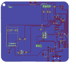
Hello everyone! I’m Enes and am hoping some of you folks may help me. I have this project for my graduation and I just wanted to be 100% sure before sending it to China for manufacturing - its my first time with PCBs O_O. It takes 3 weeks to arrive my country therefore I don’t have time to test it, I only got one shot. My prototype works perfectly on breadboard. This is the dropbox link to my BRD files and some screenshot for you guys to check it real quick: https://www.dropbox.com/sh/fnw6stdh0xfbn68/AAAU6FnlHMEo3R6zZJQOSzH3a?dl=0

I have few questions below, and I really do appreciate if you download them and control it.

1- Transmission traces between FT232 and Atmega328 are not short traces. Are these traces going to cause any trouble?
2- Did I place the decoupling capacitors correctly in my layout?
3- Is 16mil drill size too small for manufacturing?
4- Do I need to add a diode between LM3940 and ESP8266-1 ?

Thanks a lot and have a great forum.
 

Attachments

  • mycircuit.zip
    761.3 KB · Views: 100

Hi,

I'm sorry...but there are a lot of errors.
I need some time to analyze them all.

Klaus
 

Hi,

1) no problem
2) SEEMS ok
3) no problem
4) wich signal? Why?

*****
There are really a lot of issues. Some are just not nice, but some will make your project to fail - in different cases.


*****
Transmitter schematic:
* R1 has the same signal on both sides.
* DS18B20_VCC is connected to GND
* FT232_TEST is not connected to GND
* Use GND symbols (from EAGLE libraray) instead of the earth-symbols named "COM". Use "GND" as signal name.
* use meaningful names like "WIFI_RXD" instead of "D9". Btw: why "D9"?
* an LED at the SCK line may influence signal voltage levels, especially with weak signals coming from the programmer. rethink this.
* T2 connection is wrong. Maybe you need a PNP.
* a diode between VUSB and +5V violates USB specifications (but it may work)
* what is CBUS0 connection good for?
* what is DTR# connection good for? It may violate IC specifications.
* remind to include debouncing with pushbutton inputs. Either in hardware or in software.
* pusbutton on MOSI may create short circuit during programming.

Layout:
the first view:
* it seems you build your own packages. No good idea. SMD origins need to be in the center of the device. This is the point where the pick-and-place machine holds and rotates the device.
* really not nice: You didn´t route the traces in 45° / 90° angles. Even the PCB dimensions are not 90°. --> select the correct grid and the correct bend-style you you have less work with better results.
* You didn´t take care of clearances between outline, traces, device placements
* Your GND isn´t GND. It is called COM. On the bottom a big plane (that is good), but only connecte to some THM pads. No connection to the vias.
--> use GND only on the bottom side. Name it "GND" and use GND symbols in the schematic. keep all other traces at bottom side short to get a solid GND plane. Use vias to connect the device´s GND at the top side. Don´t use copper pour at the top side, use it oly for traces. (My personal taste)
* place your parts before you route the first wire. My taste: In your case it seems the ICSP connector is the most important, because it is placed in the center of the PCB and the ICs are squased at the edge of the PCB.
* You may avoid a lot of vias in the signal lines by just moving the traces. Use vias connect to GND plane instead.
* read about wifi module: Is it allowed to place it (the antenna) over a GND plane? Maybe you need to place the antenna to the PCB edge
* the routing really is a mess.

****
Receiver ... later.

Klaus
 
Second everything Klaus has said. Look carefully at a design and spend your time on placement, try different placement schemes and see how they route, its a project for a course so don't rush it.
For footprints and grids look at information on IPC-7351 and this...
https://www.circuitinsight.com/pdf/universal_pcb_design_grid_system_ipc.pdf

Look around this site I and many others have put up basic links and guides to PCB design as How do I start PCB design is a regular question.
 

Hi,

I´ve made an example how to generate a solid GND plane. With minimized traces on the bottom side.
This is not meant to be a perfect layout. I didn´t correct all the issues.
transm1.png
It just should show how I achieved the result:

* Moved traces
* moved devices
* swapped gates
* removed crossings
* removed vias in the signal lines
* added the GND vias with short traces at the TOP side

There´s no need to do the same. Some changes you will find useful, some not.


Klaus
 
Thank you so much KlausSt for all your comments i will try to fix these problems and ask my questions i am looking forward for your review of reciever
 

--i did not notice the thing about r1 thank you.
--i have found that one and it was working fine in breadboard. But you think still it is not good to use that, i will change.


--Test pin linked to ground thank you
--Use "GND" as signal name. did you mean "COM" ?
--:D i made d9 because it comes 9th digital pin of arduino but you are right they should have meaningful names.
-- okay i will remove that led i dont need it
-- does npn make more sense when you consider the way of current?
--Why it violates usb specifications because of voltage drop ?
-- i really dont know because i import that schematic from arduino web site it is schematic of arduino nano and it was like that there.
-- dont know from same reason but i will check ic specifications
-- i will keep it in mind thank you for reminding
-- i will change with another digital i/o

layout
is it not good to use both top and bottom layer as ground layer ?
generally i will work on layout to make it better thanks for all your comments
 
Last edited by a moderator:

Hi,

DS18B20: Your circuit is correct. I just saw thatone pin is named GND, the other VDD. It is very unlikely that VDD is connected to GND. But in this case it is possible.

GND: I recommend to keep on standards. Naming "COM" to "GND" just avoids confusion. It has no electrical effect as long as there are no aiutomatically routed "power" pins.

NPN: it simply doesn't work the way you drawn it.

USB: read the FTDI datasheet. Current consumption in various USB states.
CBUSx, DTR: keep on FTDI datasheet.
Btw: please add all capacitors like mentioned in the FTDI datasheet.

GND: definitely one solid plane, without cuts (like in post#5), is way better. It ensures stable GND conditions, low impedance, return path for each signal at the top layer, reduces EMI, improves EMC.
With a real solid GND plane some use additional copper pour...i can see no benefit in it.

GND: you tried connect both sides GND with vias, but the vias were isolated...no connection. In either way you need to "name" the vias with the signal name to get a connection. "COM" in your case.
Try this: print out both layers independently on paper. Use a knife and cut everywhere the gnd plane is cut. Then use tiny points of glue everywhere you have a "GND" connecting via, glueing both papers together. You will see that one sheet of paper is more stable than your two glued, but cut papers. Especially some sections will be very fragile.

Or see it like this:
* a solid GND plane is like concrete ground.
* a wire is like a rope.
* a copper pour is like a spider web of ropes. And the stability depend on how often and where the ropes are joined (vias).

Klaus
 
KlausST i redesigned my pcb schematic and layout according to your comments. Thank you so much for all suggestions and warnings. However i have some questions in my mind i wanna share

-"an LED at the SCK line may influence signal voltage levels, especially with weak signals coming from the programmer. rethink this."
i did not remove that led because all arduinos have led which connected to digital13/sck pin it shouldnt be a problem. However i increased the resistor value connected to that led to decrease the current consumption of atmega
-"* what is CBUS0 connection good for? "
Factory default configuration is RXLED# for that pin. But i did not need that led that's why i removed the led.However i didnt remove the +5v connection and resistor because i dont know how does it work? probably when ft232rl recieve data that pin becomes logic 0 and led becomes active. but it is just a prediction. Does it change anything if i remove that +5v and resistor ?
-"what is DTR# connection good for? It may violate IC specifications. "
in datasheet it is written "Data Terminal Ready Control Output" for dtr# pin i dont know what does it mean but again schematic of arduino nano is like that that's why i did not wanna change it.
-what can i do to prevent debounching of pushbuttons in hardware ?
 

Hi,

LED on SCK: I know that the AVR can drive a LED. My concern is the programmer. It is unknown. Programmers may have weaker drivers, longer cabling, series resistors... Generally I don't think any reasonable unsymmetric load at a clock pin may cause problems.
But you are free to do what you want.

Arduino: It seems the arduino designers don't care much about specifications, signal quality and reliability. Arduinos are cheap, for hobbyists and not for industrial applications. The designers save some components (a simple, cheap bjt to drive the LED) and risk reliability.

CBUS0: disconnecting the LED but connecting the remaining resistor is like saying: I don't need that much speed of my car, therefore i press the gas pedal to the limit and the same time use the brake to slow down.....
It's just a waste of power (I even think the current is off specification) and no benefit. Totally useless.

Designing electronics is not a "prediction". You have datasheets, they tell you the facts.

DTR. Function is written in the FTDI datasheet, wikipedia, and million other documents in the internet.
A capacitor in series to a switched signal may shift the voltage levels. Up to twice the initial level. Therefore it violates the specification. It may cause to hurt the isolation barrier of inputs. It may work for many years. But if your application fails after months or weeks, then don't blame it on the circuits. (Violating input voltage specifications is known to cause fail after a long time, it doesn't cause immediate fail)

Debouncing: a simple search in this forum may give many, many results. More results on a internet search.

***
I know: For a graduation project you don't need reliability. But later you will need to know how to design reliable circuits.
Datasheets tell you how...

Klaus
 
I changed everything like you said except removing that diode between Vusb and +5v. Also dtr# connection is still same because i really dont understand the relation between arduino reset pin and ftdi dtr# pin. Also i will add ftdi capacitors according to datasheet but now i wanna upload the new schematic and layout of transmitter. how does it look so far ?
 

Attachments

  • transmitter.zip
    51.7 KB · Views: 102

Hi,

maybe you sent the wrong files...

I changed everything like you said except ....

* 0°/45°/90°
* FTDI TEST pin (it won´t work)
* FTDI capacitors (it won´t work reliably)
* TOP copper pour, unconnected it is definitely worse than without pour (expect EMI problems)
* unused vias
* clearances (expect problems when PCB is produced)
* device placement, device origins (expect problems with automatic assembly)

I stop here, I´m not sure if the list is complete.

Klaus
 

    V

    Points: 2
    Helpful Answer Positive Rating
i tried to make the angles between 45 degree and 90 degree. maybe i should study geometry :D are there lots of wrong angles connections because i really dont know which one is wrong?
test pin is done
capacitors done.
To fix the copper pour unconnected issue what do i need to do. Is it okay if i make the dimensions bigger and connect the copper pour from edges ?
clearance is at least 0.2mm 8mil i did not get any errors from drc. Do you think should i increased the min clearance ?
i am gonna fix it soon especially for ftdi and atmega. Also some of capacitors have that problem their origin point is one of their side.Is it also a problem for capacitors.

I know i bothered you so much but it is really important for me and you know education in school doesnt teach that stuffs and it is my first design i know some of my questions might be dumb and silly. Thank you for helping me anyway
 

Hi,

angles: EAGLE does this for you. You just have to use the right mouse button during "route" or "wire". (As said before: It is less work to wire 0/45/90 angles than arbitrary angles)
--> In most cases it won´t harm function. The traces just look awful. In some cases you might get mechanical problems with your "out of angles" dimensions. None of your outline dimensions is 0° nor 90°.

An example how to draw the PCB dimensions:
setup:
Code:
grid mm; 
layer dim; 
miter 0; 
change width 0.1; 
set wire_bend 0;

Then draw the dimension:
Code:
wire (0 0) (82 76) (0 0);

You can copy the codes into the command line and press execute. Alternatively you can do all this with the mouse, too.

Wich trace angle is wrong tells you the DRC (with the "check angles" enabled in the tab "misc") . Hopefully you used it before.

FTDI. TEST and capacitors: Now? But not in the given data of post#11!

Copper pour: from post#8:
In either way you need to "name" the vias with the signal name to get a connection.
It has nothing to do with dimensions.

I meant clearance between outline_dimensions and copper (wires, polygon). In EAGLE it is called "Distance".
Design recommendations say you should use DRC-Distance-Copper/Dimension = 100 mil

Origin of SMDs out of center: It makes automatic assembling impossible, becuse the devices are placed at the wrong position.

****
First PCB project.
The safe way is to use EAGLE libraries. Less work, less mistakes. Almost any device is available. Look at farnell or at EAGLE internet site.
If you really want your own packages then copy existing packages and modify them as you like.
If you really need to draw new packages you first have to learn how to do it.

There are a lot of good EAGLE tutorials.

Klaus
 
design and schematic should be better now. I am gonna post it but i know still there are some mistakes. I think i will keep that dtr connection like that i dont know the purpose but i have checked lots of ftr232rl atmega328 circuit from google and lots of them were similar. In the datasheet of ft232rl there is one 10nF capacitor between Vusb and ground and after that there is ferrite bead may be i should add ferrite bead instead of diode ? and in datasheet after ferrite bead there are 4.7uF and 0.1uF decoupling capacitors. I am already using them but i did not add 10 nF capacitors but if you say replace diode with ferrite bead i will change it and add capacitor. I think dimensions and angles should be okay also. Another question is that i wanna place leds and button near to the edges but 100 mil clearance does not allow that ? Is it okay if i make the clearance smaller ? I have changed the footprint of atmega and ft232rl but there are some capacitors and leds dont have origin point in the center of them. Is it also a problem for these components ? If it is i will change it for sure. Also does lm3940 regulator need to be close to esp8266 ? Today one guy told me it has to be near to esp8266 also that guy said my sw2 circuit is wrong ? I have googled it and there are some circuits like mine. But he thinks using pull down resistor is not correct he said there should be pull up. I am gonna stick with you about everything because he is not that reliable. Also he said it is not good to use resinator because it is hard to find ? is it really hard to find ? And again sorry copper pour issue is still not that clear for me when you say TOP copper pour, unconnected you mean names of vias are not the same with its traces ? if that's what you meant they also should be connected now i am gonna upload the new design i hope this time it is better. :-?
 

Attachments

  • transmitter0.1.zip
    52.4 KB · Views: 86

Hi,

I've searched about the DTR capacitor. It is a quick-and-dirty solution for the arduino bootloader to reset the AVR. I don't recommend this (without additional protection circuit) for reliable applications.

Ferrit bead: it is for EMI/EMC purpose. It is between USB connector and FT232 supply. Your diode is elsewhere, therefore it makes no sense to replace them.

LED placement: If you are in doubt you have to talk to the SMD assembling/soldering company.

Capacitor origins: read post #14

LM3940 to ESP8266 distance. It can be meters, but:
* you need to take care about voltage drop. Voltage drop depends on resistance and current. For low resustance you need thick traces.
* you need to take care about (high frequency) impedance. With a bulk capacitor in parallel a fast ceramics capacitor at both devices you should be safe.

SW2: I already commented it at post#3. I don't know it's purpose, therefore I can't decide if it is funcionally wrong. You need to give more information about that.

Resonator: It is cheaper than an Xtal. That's it. Availability depend on the location where you live...

Copper pour. Later. Currently I'm working on a tablet without EAGLE.

Klaus
 
Hi,

Schematic:
* There are still all recommended capacitors missig at the FTDI chip. PLEASE read the datasheet and follow the ruels. You really risk that your circuit fails.
I will ignore them in future.

Board:
It looks more tidy now. And the bottom GND plane is very solid. :)

I ignore now the DRC violations regarding outline/dimension. I assume you know what you do.
I ignore now the mistakes made in the libraries.

Copper pour on TOP side.
You ask.. therefore I try to explain again:
* It is not connected to a signal. It is not "GND" it is not "COM" it is just floating.
* floating copper pour is definitely worse than no copper pour.
* especially bad regarding EMI/EMC are the nasty orphans.

If you ask me: I´d delete the complete TOP copper pour.

May I ask, why you insist on the copper pour?

There is a via next to the ICSP connector. It is useless. You see it is not connected to the TOp copper nor it is connected to BOTTOM copper. It´s just a plated hole, isolated to anything.

Now you have 6 wires in the dimension layer. Temporarily move the right bottom corner to see the hidden two. Remove them to avoid problems at PCB production.

Not wrong, but not nice, too. The 3V3 connection to the ESP. I talk about the horizontal trace, unnecessarily fed to the bottom, then after some mm it is fed to the top again. A single via will do.
(If you rotate T2 90° CW then you can do without via)
Btw: T2 is THM. Why not SMD. BC847.

Klaus
 
Hey
Thank you for warning about capacitors tonight i am gonna add them :D Also Should i add more 0.1uF capacitors for atmega328 ? because again someone said it is needed ?
Now i get what you mean unconnected copper pour :D sorry about late understanding can i use that plane as a power plane or something like that if it is not that good about EMC please tell me i have no problem about removing it. And again thank you for warning 6 wires in dimension layer i will fix it
 

Hi,

Also Should i add more 0.1uF capacitors for atmega328 ?
simple answer that is valid for the future: consult the datasheet.
It is the more reliable source of information. (If I recommend something other than given in the datasheet, then if you are in doubt please keep on the datasheet)

***
Copper pour: for sure you can use it as power plane. But it is not necessary.

It is way more important that you have a sloid GND plane. Because every supply and every voltage measuremetn refers to it.
The VCC wires just need to be low ohmic (DC resistance) so that the voltage drop across the wire is well within specifications.
Here check the 3V3 line to the ESP01. It may draw several 100mA.
Your wire is about 60mm long, 0.4mm wide and 35um thick I assume. This means a resistance of about 80mOhms.

Let´s say 200mA x 0.08 Ohms gives a voltage drop of about 16mV. Well within specification. No thing to worry about.

Your signal lines are 0.4mm wide also, but they carry about no current.
For my taste they are realtively wide. (they could be 0.1mm wide. But no need to change it)

If you want to adjust trace width, then the width of the 3V3 lines. Especially to the ESP01.

This additionally is an "optical" benefit for the supply lines to be in contrast to signal traces.

Klaus
 
Hey :) today i need to send my gerber files to manufacturer. I cant do that without getting your confirmation. If i do someting wrong it will take 3 more weeks to get that pcbs. So thank you too much for your all effort.
-In transmitter There are two switch one of them for reseting atmega other one is clearing the eeprom.
-In reciever there are two different switch one of them is again deleting eeprom of atmega328.Other one is Changin mode of the device i mean that switch turn on/off the relay.
-If is there any mistake please let me know and again i wanna say thank you.
 

Attachments

  • soncizim.zip
    117 KB · Views: 99

Status
Not open for further replies.

Part and Inventory Search

Welcome to EDABoard.com

Sponsor

Back
Top