Continue to Site

Welcome to EDAboard.com

Welcome to our site! EDAboard.com is an international Electronics Discussion Forum focused on EDA software, circuits, schematics, books, theory, papers, asic, pld, 8051, DSP, Network, RF, Analog Design, PCB, Service Manuals... and a whole lot more! To participate you need to register. Registration is free. Click here to register now.

Smaller die size by tighter SPICE corners?

Status
Not open for further replies.

Macduff

Newbie level 2
Newbie level 2
Joined
Jan 8, 2020
Messages
2
Helped
0
Reputation
0
Reaction score
0
Trophy points
1
Activity points
20
Hi all,

Firstly, I'm a foundry process engineer, with very limited knowledge about circuit design. My question could be silly. Please kindly give me indications easier to understand. :)

I'm told that good process variation control can save chip size, but I don't really know the reason. I guess it could be associated with timing. For instance, tighter SPICE corners can shorten necessary setup time or hold time, then designers can use smaller width devices or less delay cells. Is my guess close to the answer?

Thanks!
 

The more control you have over your process, the more "deterministic" the outcome will be. You wouldn't have to overdesign your circuit to cover all outliers due to the process variations. And would eventually boil down to a smaller design. Sounds like a reasonable assumption.

From an analog point of view, it is pretty well established [Pelgrom et al] that the matching is inverse-proportional to the area of your devices. With tighter control, the area can thus be made smaller.
 
Hi jjx,

Thanks for the asnwer. Is it possible that you can give one simple exampe of "overdesign of the circuit"? Or few key words will be fine. I can google and study it myself. Thanks again!!
 

Not that many keywords on the top of my head. I am just arguing that if you want to design a transistor with a certain driving strength to meet e.g. setup/hold times for FF corner as well as SS corner. Say that FF would give you a required size of 1 and SS would give you a required size of 3. The tighter FF and SS requirements are, the lower the span between 1 and 3 would be. It's about the design margin.

Perhaps buzz words could be overdesign, area, yield, design margin, die size
 

Not so much a thing for digital, but a big deal for analog.
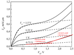
Consider a case where (say) you have an "edgy" process
flirting with impact ionization at shorter L. Your modeling
folks might manage to express this "distribution" properly.
Or not.

In the better case, that they do, you might see the "drain
curl" affect your op amp gain stage. As Av=gm*Ro, this will
be a factor of 3-10 (10-20dB) degradation to your stage
gain at higher drain voltage.

ImpactIonization2.png

If you are tasked to make a 70dB AVOL op amp and this
gives you 50dB, even cascoded, your only next choice is
to move to a multiple-gain-stage topology. This is not only
larger by transistor count, it's also likely much more difficult
(and needful of much greated compensation-capacitor area)
to stabilize.

Now the question is not only SPICE corners - here you
only ask for realism / "fair warning". The real question as
OP asked, is about process control of device attributes.

For an analog application designers would really like drain
linearity - not really a top-line process control param,
more like something you'd get at by meta-analysis (like
a pair of ID-VD curves in subthreshold where you live,
looking at whether ID is constant slope or curved / kinked).
I haven't seen this depth in WAT data / programs myself.
But I have been surprised on occasion by the effects
that go unmodeled, ruining performance relative to
simulated.

If your process control had a better grip on Leff, on
spacer / LDD / halo strength at suppressing II, the
"drain curl" might be suppressed and enable much better
/ smaller analog block design (or at least push out the
"pain threshold"). Maybe your analog blocks can make
75dB (WC) rather than 40dB and now applications up
to 70dB (say, for gain error in A=100 CL) are able to
use the simplest, smallest op amp design instead of a
2V transistor count, 4X area two-gain-stage design.

In cases where this dominates (like say a ROIC with
a million pixels each with its own TIA, and a demand
for high photon-to-bits linearity across a 12-bit range)
the effect could be not just die size, but success or
failure - die size being "pinned" by the detector-plane
design, that you're told to accept. Can you fit 20
transistors and 5pF of MOS cap in the pixel extents?
While getting TIA gain consistent with a sub-LSB
(12 bit) gain error?
 

Status
Not open for further replies.

Part and Inventory Search

Welcome to EDABoard.com

Sponsor

Back
Top