Continue to Site

Welcome to EDAboard.com

Welcome to our site! EDAboard.com is an international Electronics Discussion Forum focused on EDA software, circuits, schematics, books, theory, papers, asic, pld, 8051, DSP, Network, RF, Analog Design, PCB, Service Manuals... and a whole lot more! To participate you need to register. Registration is free. Click here to register now.

SMA connector regarding PCB design & layout

Status
Not open for further replies.

samiran_dam

Full Member level 2
Full Member level 2
Joined
Apr 17, 2010
Messages
122
Helped
3
Reputation
6
Reaction score
3
Trophy points
1,298
Activity points
2,419
Dear All,

I am new to PCB design and layout. Currently I designing the PCB for testing my design prototype. For this purpose, I need to place a thru-hole SMA connector.

However, I dont know -

1. Which part to use in the Capture schematic for the SMA connector.
2. Which footprint to be used.​

F4683306-01.jpg


Please help.

Thanks
Samiran.
 
Last edited by a moderator:

Hi

I think when no part exists in the PCB design software used, you unfortunately have to design it yourself - it looks easy once you know how, I never have. Same goes for the footprint, they seem to be linked in the program I use for schematics, so once you've done one the second stage (i.e. footprint) takes up less time.

Your SMA connector datasheet will have a specific footprint for your specific connector, and if no datasheet is available then try with a good ruler/(digital) caliper (if you're lucky enough to have one, especially digital) to get reasonably precise measurements. A set of stiff compasses can be an okay makeshift caliper for measurements, if desperate.

Good luck.
 

The component footprint for this is 5 pads and a square surrounding them.
It's not hard to do, find the datasheet for the correct dimensions and learn to use your pcb packages so that you can make your own footprints.

Its simple, honest.

If you really, really, really struggle to make a footprint that only has 5 simple pads in then go to pcblibraries.com and download the library expert lite which (for free, free, free) will enable you to enter the component dimensions and output a footprint in your cad package format that you then can import into your library.
But (there is always a "but") you will need to learn how to use this new tool, just like you need to learn how to make very simple footprints in your cad package.

How about we concentrate on that?
What can you not do? when you try what difficulty do you have?

Watch this video, when you cannot figure out what you are to do then come back here (please do) and let us know and we can guide you further :)
https://www.youtube.com/watch?v=0ZcgduOr9gk And if your not using Eagle then let us know which cad package you are using. (I just guessed)
 
Last edited:

The component footprint for this is 5 pads and a square surrounding them.
It's not hard to do, find the datasheet for the correct dimensions and learn to use your pcb packages so that you can make your own footprints.

Its simple, honest.

If you really, really, really struggle to make a footprint that only has 5 simple pads in then go to pcblibraries.com and download the library expert lite which (for free, free, free) will enable you to enter the component dimensions and output a footprint in your cad package format that you then can import into your library.
But (there is always a "but") you will need to learn how to use this new tool, just like you need to learn how to make very simple footprints in your cad package.

How about we concentrate on that?
What can you not do? when you try what difficulty do you have?

Watch this video, when you cannot figure out what you are to do then come back here (please do) and let us know and we can guide you further :)
https://www.youtube.com/watch?v=0ZcgduOr9gk And if your not using Eagle then let us know which cad package you are using. (I just guessed)

Dear Mattylad,

Many many thanks for your kind concern. Basically, I am using OrCAD 9.2. I have made footprints of few custom components which will be used in the PCB. However, assuming that SMA connector is a very common component being used in PCB, I thought its footprint may have been available in the library. And guess what? I have found one ready footprint (RF/SMA/V) for SMA connector. So, for the time being I will use that. However, I have downloaded the software you pointed and definitely I shall give it a try to use that one in future in case I need a quick solution. Thanks a lot.

Thanks
Samiran.
 

Most PCB CAD packages come with extensive libraries, they may list thousands of parts\footprints.

However 98%of the time you can guarantee that the one that you really want is not there - murphys law lol
 

This kind of footprint is easy to create.You need to check SMA's datasheet and find the "recommend / suggest PAD loyout".
Be more care about the hole size and distance.
By the way,the holes outside are connect to GND,you'd better design a thermal PAD.Please see the picture attached below.
1111111.jpg
 

By the way,the holes outside are connect to GND,you'd better design a thermal PAD.Please see the picture attached below.
Not so simple, unfortunately. The extra inductance may be inacceptable for a RF design. Similar problem with high current through plated components.
 

In that connector they do not want thermal relief, use a higher wattage iron to solder it.
Get it right first time as it will be a PITA to remove.
 

SMA.png
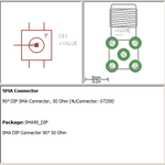
I've been using this 90 degree SMA connector for some of my designs. Its got the same pin spacing/pitch as a vertical one. Look for adafruit eagle library and you'll find it.
 

Status
Not open for further replies.

Part and Inventory Search

Welcome to EDABoard.com

Sponsor

Back
Top