Continue to Site

Welcome to EDAboard.com

Welcome to our site! EDAboard.com is an international Electronics Discussion Forum focused on EDA software, circuits, schematics, books, theory, papers, asic, pld, 8051, DSP, Network, RF, Analog Design, PCB, Service Manuals... and a whole lot more! To participate you need to register. Registration is free. Click here to register now.

Slope compensation requirements

Status
Not open for further replies.

mtwieg

Advanced Member level 6
Joined
Jan 20, 2011
Messages
3,897
Helped
1,311
Reputation
2,628
Reaction score
1,433
Trophy points
1,393
Activity points
29,936
Hello, I'm in the process of debugging a LT3436 boost converter and came across the following in its datasheet:
The slope compensation circuit within the LT3436
prevents subharmonic oscillation for inductor ripple currents
of up to 1.4AP-P,
Now, I know what subharmonic oscillation and slope compensation are, but I recall that the slope compensation is based on the downward slope of the inductor current during the off time. But here the datasheet specifies it based on the magnitude of the ripple (regardless of the input and output voltage, and thus regardless of the slopes). It does not say anything about the waveform added by their slope compensation. So I'm trying to figure out what's going on here... but I'm unable to find a resource that gives the gory details of slope compensation. I'm hoping to figure out where that 1.4App number comes from.

I'm concerned about this because I'm seeing bizarre instabilities in the LT3436 supply, even though I should be very well compensated and I should be operating below 50% duty cycle. It see waveforms that look like some sort of burst mode operation, though this chip isn't specified to have that capability. So I strongly suspect there's something going on inside the thing that isn't well described by the datasheet, like a variable slope compensation scheme.

Thanks in advance,
-Mike
 

Hi Mike,

Is the burst mode happening even at high load conditions?

Normally, burst mode happens at light load conditions, this
is because your output capacitor isn't discharging much
during the switching cycle. Your voltage loop, even though
you are using a current mode controller, is preventing
it to give a pulse. The controller will wait until the
output level falls to a certain value before it gives
another burst. And when the load current is enough,
current mode will kick-in.

You also said that you are only operating at <50% duty.
Slope compensation, as far as I know, is only required
if you operate beyond 50%.

For you reference, I suggest you to read the document from the link below...


https://www.venable.biz/tp-05.pdf


Best Regards,
Leo
 

I bet the 1.4A pertains to some saturation of a current sense circuit, or
something like that.

I've seen subharmonic problems from package design / pinout (bond
wire coupling) requiring full chip relayout, something like this may be
at play at board /module level.

I've seen some good concise explanations in the app notes / datasheets
for the old Unitrode UC38xx PWMs. Though integrated converters may
take other approaches than stuffing current onto the ramp (we put a
VOUT dependent bias onto our current sense signal, in an integrated
buck).
 

Hi Mike,

Is the burst mode happening even at high load conditions?
It happens at light load, but only when the input and output voltages are within certain ranges. if Vout/Vin is low it tends to start bursting, but not when Vout/Vin is greater than 4/3.

I also see it sometimes at heavier loads, when the supply is operating in CCM. It looks like a genuine loop oscillation, but I can't figure out why it would oscillate at a frequency above my crossover point.
Normally, burst mode happens at light load conditions, this
is because your output capacitor isn't discharging much
during the switching cycle. Your voltage loop, even though
you are using a current mode controller, is preventing
it to give a pulse. The controller will wait until the
output level falls to a certain value before it gives
another burst. And when the load current is enough,
current mode will kick-in.
I know what burst mode is; I use a lot of Linear Tech parts and they often integrate it. But it's not specified at all for this controller. It shouldn't have a burst mode.
You also said that you are only operating at <50% duty.
Slope compensation, as far as I know, is only required
if you operate beyond 50%.
If the slope compensation is a simple ramp and summing circuit, then this is true. But I suspect that the amount of slope compensation is not fixed within the IC, or that it is being enabled and disabled, which is causing the bursting.
For you reference, I suggest you to read the document from the link below...


https://www.venable.biz/tp-05.pdf


Best Regards,
Leo
I've already read all of venable's app notes, thanks. I'm looking for a more quantitative analysis of slope compensation, not some rules of thumb.

---------- Post added at 20:04 ---------- Previous post was at 19:57 ----------

I bet the 1.4A pertains to some saturation of a current sense circuit, or
something like that.
That might make sense if it were specifying a peak current level, but it's specifying the peak to peak ripple current. The converter is designed to operate with switch currents up to 3 amps (and I've verified I can draw that much).
I've seen subharmonic problems from package design / pinout (bond
wire coupling) requiring full chip relayout, something like this may be
at play at board /module level.

I've seen some good concise explanations in the app notes / datasheets
for the old Unitrode UC38xx PWMs.
I've never seen a unitrode chip with slope compensation internally. I've used some of their controllers and the results were always nice, probably because everything about it was completely specified and easy to model. I kind of wanted to avoid having twenty external components though, which is why I went for this part... but I'm starting to regret it.
Though integrated converters may
take other approaches than stuffing current onto the ramp (we put a
VOUT dependent bias onto our current sense signal, in an integrated
buck).
Interesting. How does a DC bias stop subharmonic oscillation though?
 

Hi Mike,

May I ask, why are you worrying about the burst operation?
You said that it only happens at light load and/or when
Vout/Vin is low. Low Vout/Vin means you have low duty cycle.
This time, your Inductor voltage is very low and so is your inductors
ripple current. At this levels your voltage loop is doing the regulation,
not you current loop. Voltage mode means you have very slow
loop compensation, that is because your feedback is already
delayed by the LC of your plant.

In that perspective, the datasheet doesn't need to indicate that
it can operate at burst mode. Ask I've said, the controller will
not give pulse if the output is still enough.:grin:

Cheers...:razz:

Regards,
Leo
 

The general purpose of burst mode is to increase efficiency at light load, at the expense of increased output ripple. In my application I'd much rather have the lower efficiency with low ripple. Also when loading increases in between bursts, while the supply is not operating at all, the response time is drastically worse.

Basically if I knew it had burst operation I would have used a different controller.

But I'm still not absolutely convinced it's real burst mode operation, since not even the SPICE model in LTspice shows this behavior, and they usually are pretty thorough in their models.
 

My point is, if your controller is seeing high output voltage,
then it will skip few pulses before it again give another pulse.
Why will it give another pulse if it sees the output has more
than enough? That is because your loop is not very fast enough to
see the output voltage rising or has already gone higher than
the required. The controller will not give you another pulse
unless you are below the threshold. All controllers behaves
like that.

As a remedy, you need to make your voltage loop
very fast... but as i've said, you cannot do that
because of your LC circuit, there will be a delay in the sensing
that will cause your controller to give higher duty cycle than
required and that causes the output to go higher than the
required regulation voltage.

Yes, burst mode operation is to increase efficiency...
But that is for resonant mode controllers. Which will
operate the controller to its maximum switching frequency
but in short bursts.

Try to check your feedback network also,
it might be picking-up a lot of noise.
Remember that you are operating at very high frequency(800kHz).
 

Since this chip usually operates as a boost converter - the slope comp is relative to the current rise when the switch is on as opposed to a buck converter (which is different for slope comp).
The cause of instability is either layout, or the component choices for the volt loop are wrong - or both.
A careful & complete reading of the data sheet will give you the solutions, Regards, Orson Cart.
 

Orson,

I think we have the same idea, the voltage loop is causing the instabilities.
Careful tuning of the FB loop compensator might solve the problem.
 

mtwieg, it is normal for these fancy pwm controller ic's to have extremely badly written datasheets.

Thats why i always stick to the standard pwm controller ic's like uc2843 etc etc.
-and make my own protective functional circuits as extra circuitry.

The only way to get a highly integrated pwm controller ic to work, is to first build an investigative prototype so that you can reverse engineer it and find out what it really does.

The datasheet will NOT EVER tell you how these highly integrated ic's work........and the applications engineers will just tell you that it can do everything that you want.

I have seen first-off prototypes of SMPS's come out (comprising fancy pwm controller ic's) , and NOT ONE enginner in the whole dept can work out why it is going wrong.

....80 years worth of smps design experience cannot work out what is going on.

...and then we start from scratch, and spend time reverse engineering it because we have to because the datasheet is pathetic
 

I'd be extremely surprised if the voltage feedback loop is unstable. It's a current mode supply, so it should never meet the criteria for loop instability. The frequency of its RHP zero should be far outside my loops bandwidth, same with the error amplifier bandwidth...

Noise pickup doesn't seem likely, since the oscillation is very consistent, and at a much lower frequency than my switching frequency.

I'm thinking there's not much to be done about it... it's disappointing because I've had good experience with LT documentation in the past. Generally they explain what's going on in great detail. But I guess next time I'll stick with a general control IC...
 

What values have you used for the volt loop? Is your layout all SMD with tight tracking and o/p away from control lines? Have you kept the current ripple below 1.4A p-p in the design? what is Vo min and Lout? and freq?
 

What values have you used for the volt loop? Is your layout all SMD with tight tracking and o/p away from control lines? Have you kept the current ripple below 1.4A p-p in the design? what is Vo min and Lout? and freq?
Here's a schematic of the external components. In this configuration the crossover frequency should be around 5.5KHz with a phase margin around 80 degrees. It's set up for transient load testing (as I have on the bench). The inductor value is oversized if anything, and my max ripple current should be about 0.3A. All components are SMD, using low ESR ceramic capacitors. I've looked at the switching noise and it's pretty quiet. I have footprints for an RC but decided not to use them, since I'm only measuring drain overshoot of a few volts.
lt3436schem.PNG
 

thanks for the info - will have a look at it, by the way is there some decent decoupling right at the input of the booster? what is the freq of the sub-harmonic osc?
 
Last edited:

There's another ceramic 4.7uF cap on the input. There's also a typical 470uF electrolytic nearby.

Also I don't think it's a sub harmonic oscillation per se. It's something happening inside the controller which causes the peak inductor current to not smoothly track the error amp voltage. I think it may be that the internal slope compensation is turning itself on and off, or there is a burst mode function inside which effectively puts hysteresis on the error signal... or something. The frequency of the burst changes a bit, but it's normally in the range of 10-20KHz.

edit: crap, I may have figured out the cause of the instability I'm seeing at heavy loads. I don't show in that schematic that I'm using a resistor divider from the Vcc pin to the shutdown pin to act as an UVLO. The LT3436 is means to do this, and has a comparator with hysteresis for setting lockout thresholds (I have my thresholds set at about 13V and 14V). It could be that my DC bench supply is too high an impedance and the supply voltage is drooping below the threshold during load, shutting off, rising up, repeat.... basically a big relaxation oscillator. I'll have to test that next time I have the chance.
 
Last edited:

ah yes, the unknown characteristics of the source, it is always worth looking a the o/p of the power supply source (right at its terminals) to see if it is contributing something to the mix, if the power source has a 10-20kHz oscillation the boost converter will carry it to its o/p as the f/b loop can not be made fast enough to counteract it.
Your choice of feedback components seems OK, and the choke large enough (by a factor of nearly 2), hopfully it is linear up to 1.1amps (or higher if the chip freq is at the low end of 640kHz).
If it is not the power source and/or the "relaxation oscillator" inadvertently constructed, then I would try 100pF across the 1k in the Vout divider - we have found this very succesful with similar chips.
Let us all know how it goes...
 
  • Like
Reactions: mtwieg

    mtwieg

    Points: 2
    Helpful Answer Positive Rating
Well, it wasn't the UVLO... there was droop on the input during transient loading, but only a couple hundred mV max, not enough to trip it.

I just decided to take a bunch of scope captures under different line and load conditions. For these I actually changed the compensation components so that C2=10n, R2=12K, C3=220p (refer to earlier diagram). This should have given me a crossover frequency around 10KHz with a phase margin still around 80 degrees. This was my original target for bandwidth. I think I could have aimed much higher, but this supply is sourcing a gate drive transformer driver, which drives a full bridge of CM600 IGBTs at about 30KHz, so basically it has to source huge pulses of current at 30KHz, and I didn't even want to try regulating that crap.

Anyway, here are a bunch of figures. All of these are with Vin=15V, and the only thing I'm changing is the output voltage (set by a pot in the feedback loop) and a load resistance RL (which is added in parallel to the static 1.3K load which is always there, so even if I say RL=50K, the effective load is still pretty much 1.3K). All the waveforms are AC coupled, sometimes averaged to show phase shift better.
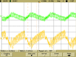
First three screens are showing the condition Vout=20V, RL=99.
First is a shot of Vout (yellow), and error amp output Vc (green). This is with averaging on. So there's already an oscillation, at over 100KHz...
print_00_Vo20_RL99_Vout_Vc.png
Same conditions, but showing Vout(yellow) and switch voltage Vd (green). You can see that the current is becoming discontinuous for a few cycles.
print_01_Vo20_RL99_Vout_Vd.png
Same conditions again, showing Vc(yellow) and switch voltage Vd (green).
print_02_Vo20_RL99_Vc_Vd.png
I would have shown all three (and inductor current) for each configuration, but I only had a 2channel scope. So for the rest of them I just show Vout on yellow and Vc on green.

Here's Vout=18V, RL=1K. Looks clean and stable
print_03_Vo18_RL1K.png

Vout=18, RL=710. Now I get some instability with ringing in it...
print_04_Vo18_RL710.png

Vout=18, RL=300. Even worse looking
print_05_Vo18_RL300.png

Vout=18, RL=100. Not it's a smooth high frequency oscillation. This is with trace averaging.
print_06_Vo18_RL300.png

Vout=21.5V, RL=50K. This is what I was thinking was "burst" mode.
print_07_Vo215_RL50K.png

Vout=21.5V, RL=1K. Again, burst frequency increases, becomes more chaotic.
print_08_Vo215_RL1k.png

Vout=21.5V, RL=400. Now it seems to be stable again...
print_09_Vo215_RL400.png
 
Last edited:

Continuing in new post due to attachment limitations...

Vout=21.5, RL=100. Still pretty quiet, maybe some slight oscillation.
print_10_Vo215_RL100.png

Vout=25.5, RL=50K. Burst mode again.
print_11_Vo255_RL50k.png

Vout=25.5, RL=900. More bursting.
print_15_Vo255_RL900.png

Vout=25.5, RL=500. Stable now.
print_14_Vo255_RL500.png

Vout=25.5, RL=100. Still stable, but a good amount of ripple (this is the max load out of all these).
print_13_Vo255_RL100.png

So I'm not sure what to think. In the ones with averaged traces I can see that the gain and phase from Vo to Vc is about what I'd expect. However, the signal on Vc shouldn't be able to reinforce such a large signal on Vo, given what the datasheet says about the current sense gain. I don't think the RHP zero can be screwing things up either. This suggests to me that something inside the chip isn't what I expect. Thoughts?

PS. Orson, I tried adding bits of capacitance on the feedback pin but it never helped.
 

Attachments

  • print_12_Vo255_RL1K.png
    print_12_Vo255_RL1K.png
    37.7 KB · Views: 95
Last edited:

Nice to see the real thing, the basic thing going on here is: lighter loads = less damping, heavier loads = more damping (and therefore stable) - this sort of thing is pretty common with boost converters (and Cuk converters).
Basically there are two approaches, 1, slow down and/or damp the volt feedback loop.
2, add speedup RC network across the R that goes from the o/p to the FB pin.
 
  • Like
Reactions: mtwieg

    mtwieg

    Points: 2
    Helpful Answer Positive Rating
Nice to see the real thing, the basic thing going on here is: lighter loads = less damping, heavier loads = more damping (and therefore stable) - this sort of thing is pretty common with boost converters (and Cuk converters).
Well I think to be precise I'm seeing stability with higher output voltages. Makes sense, since doing so lowers the loop gain (since I'm changing output voltage using a pot in the feedback network).
Basically there are two approaches, 1, slow down and/or damp the volt feedback loop.
I'd hate to slow it down any more.... I still see no reason why a current mode supply should be this hard to stabilize.
2, add speedup RC network across the R that goes from the o/p to the FB pin.
You mean use a type III compensation scheme? Might be feasible. The fact that I have a variable output feedback makes that a little dicey though. I might try to throw another zero in there right around 100KHz, where my oscillation is happening.

But there's still definitely some bullshit inside the chip. I can tell that just by looking at the first three pics there. In the first, you see that the output voltage is about 190mvpp at about 110KHz. The output impedance of my capacitors at that frequency should be less than 100mohm (assuming my output capacitors aren't just garbage...), so my output current should be about 1.9App at that frequency, and 2.5App on the input. But my Vc is about 50mVpp, which should only modulate the input current by 0.25A (according to the values of the current sense resistor and amplifier inside). The gain of the power stage is off by a factor of ten.... that's definitely part of the problem.
 

Status
Not open for further replies.

Similar threads

Part and Inventory Search

Welcome to EDABoard.com

Sponsor

Back
Top